Resistive Switching Behavior in Organic–Inorganic Hybrid CH3NH3PbI3-xClx Perovskite for Resistive Random Access Memory Devices
(2015) - Eun Ji Yoo, Miaoqiang Lyu, Jung-Ho Yun, Chi Jung Kang, Young Jin Choi, Lianzhou Wang
- Link:
- DOI: 10.1002/adma.201502889
- Zotero Link: Resistive Switching Behavior in Organic–Inorganic Hybrid CH3NH3PbI3-xClx Perovskite for Resistive Random Access Memory Devices
- Tags: #paper
- Cite Key: [@yooResistiveSwitchingBehavior2015]
- Linked notes: Paper Annotations
Abstract
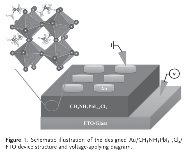
The CH3NH3PbI3-xClx organic–inorganic hybrid perovskite material demonstrates remarkable resistive switching behavior, which can be applicable in resistive random access memory devices. The simply designed Au/CH3NH3PbI3-xClx/FTO structure is fabricated by a low-temperature, solution-processable method, which exhibits remarkable bipolar resistive switching and nonvolatile properties.
Notes
Annotations (1/20/2023, 10:31:11 AM)
“Herein, we report the fi rst example of applying organic– inorganic hybrid perovskite materials in nonvolatile memory devices with a remarkable appearance of RS effect.” (Yoo et al., 2015, pp. 6,170)
“In comparison to their inorganic counterparts, one notice- able advantage of organic–inorganic hybrid perovskites lies in their facile and low-temperature processability (see the Experimental Section for details).” (Yoo et al., 2015, pp. 6,170)
“In particular, inor- ganic perovskite materials with various functionalities such as dielectric, ferroelectric, semiconducting, and light-sensitive properties are of great interest for RRAM application. ABO 3 - type ceramic perovskite compounds such as BaTiO 3 , SrRuO 3 , SrZO 3 , and Pr 1-x Ca x MnO 3 have been widely investigated in RRAM applications in single or multijunction architectures with a noticeable RS effect, resulting in multilevel tunability of resistance state, a bipolar switching property, and light-/ temperature-/magnetic-fi eld-induced behavior. [ 7–10 ]” (Yoo et al., 2015, pp. 6,170)
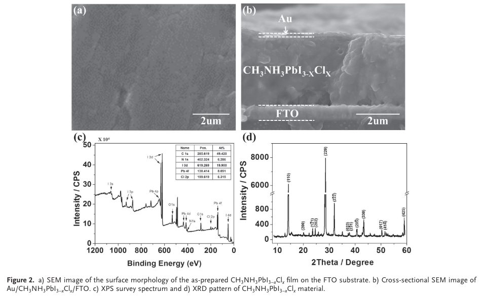
“Energy-dispersive X-ray spectroscopy (EDS) measurements have been further conducted to confi rm the elemental compositions of CH 3 NH 3 PbI 3-x Cl x fi lm (Figure S3, Supporting Information). These XPS and EDS analyses clearly demonstrate that the CH 3 NH 3 PbI 3-x Cl x has a well-defi ned stoi- chiometry. X-ray diffraction (XRD) measurements were used to verify the crystallization of the perovskite fi lm, as shown in Figure 2 d. The very sharp peaks indexed as (110), (220), and” (Yoo et al., 2015, pp. 6,171)
“Note that some very small peaks in the XRD pattern may be associated with trace amounts of impurities of PbI 2 , CH 3 NH 3 PbCl 3 , and CH 3 NH 3 I, which have been commonly found in Cl-doped perovskite fi lms, which has been reported previously in the literature. [ 20b ]” (Yoo et al., 2015, pp. 6,171)
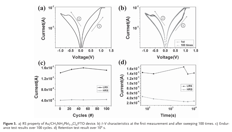
“Figure 3 a presents typical I – V characteristics of the Au/ CH 3 NH 3 PbI 3-x Cl x /FTO device under the voltage sweep of 0 V → 1 V → 0 V → -1 V → 0 V. When an external voltage is swept from 0 to 1 V, the resistance transition from high- resistance state (HRS) to low-resistance state (LRS) is observed at ≈0.8 V, which means the set process occurs.” (Yoo et al., 2015, pp. 6,171)
“After this transition, the LRS remains until the negative bias voltage is applied. The resistive state returns to the HRS at ≈-0.6 V, corre- sponding to the reset process. The set and reset processes occur at opposite bias polarities, indicating that the device has bipolar RS characteristics.” (Yoo et al., 2015, pp. 6,171)
“As shown in Figure 3 d, the HRS and LRS values measured at the 0.25 V are almost unchanged over the time period of ≈10 4 s.” (Yoo et al., 2015, pp. 6,171)
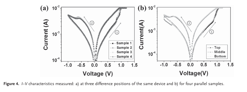
“The set voltages of each position are measured to be 0.86 V (top), 0.90 V (centre), and 0.86 V (bottom), and the reset voltages of each position are measured to be -0.65 V (top), -0.63 V (centre), and -0.60 V (bottom), respectively. Deviations of the set and the reset volt- ages at the three positions are in the range of ±0.05 V” (Yoo et al., 2015, pp. 6,172)
“It is clear that the CH 3 NH 3 PbI 3-x Cl x fi lms with different thicknesses (the results of the 2.5 µm sample are shown in Figure 2 b) all exhibit a typical RS effect (Figure S7, Supporting Information). Inter- estingly, the operating voltage decreases from 1 to 0.5 V as the fi lm thickness decreases from 2.5 to 1 µm.” (Yoo et al., 2015, pp. 6,172)
“21 ] where the switching layers can be fabricated by various methods including drop-coating, spin-coating, and printing techniques. [ 22 ]” (Yoo et al., 2015, pp. 6,173)
“In this study, for the Au/CH 3 NH 3 PbI 3-x Cl x /FTO devices annealed at various temperatures (30, 40, 50, 60, 70, and 80 °C, respectively), the I – V curves were all measured in air ( Figure 5 ). It is clear that despite slight variations, a repro- ducible RS behavior is observed in the temperature range from 30 to 80 °C. These results demonstrate that our devices are thermally stable to operate in the above-mentioned tempera- ture range, which is important for memory device applications.” (Yoo et al., 2015, pp. 6,173)
“It is of importance to compare the RRAM key param- eters of the CH 3 NH 3 PbI 3-x Cl x based device with those pre- pared by commonly used oxide counterparts.” (Yoo et al., 2015, pp. 6,173)
“It is well known that defects, for example halide vacancies, can be readily formed in the CH 3 NH 3 PbI 3-x Cl x fi lm during the solution-based fi lm-dep- osition process, which may subsequently play a role as charge- carrier trapping sites [ 25–27 ] It is thus expected that the main con- duction mechanism in our device would be the trap controlled SCLC by the defects inside the CH 3 NH 3 PbI 3-x Cl x . To verify this hypothesis, we further conducted photoluminescence (PL) measurement , which is a useful tool to investigate the presence of defects in the CH 3 NH 3 PbI 3-x Cl x materials. [ 2” (Yoo et al., 2015, pp. 6,173)
“28,29 ]” (Yoo et al., 2015, pp. 6,173)
“the charge recombination lifetime in the CH 3 NH 3 PbI 3-x Cl x fi lm based on the PL decay measurement results is estimated to be very short, 84.6 ns, sug- gesting that the defects (trap states) in the CH 3 NH 3 PbI 3-x Cl x fi lm can easily capture the charges generated by pulsed laser illumination.” (Yoo et al., 2015, pp. 6,173)
“The bulk trap generation as the major conduction mechanism can be also confi rmed from a much higher bulk resistance of CH 3 NH 3 PbI 3-x Cl x than the contact resistance between top electrode (Au) and CH 3 NH 3 PbI 3-x Cl x .” (Yoo et al., 2015, pp. 6,173)
“To further understand the conduction mechanism, we replotted the I – V curves in a log– log scale as shown in Figure S10a (Supporting Information). The red arrow indicates the sweeping direction. Based on the fi tting results, three different slopes have been observed in the HRS and LRS regions, which refer to ohmic, bulk-controlled including Poole–Frenkel (PF), and SCLC conduction, respec- tively.” (Yoo et al., 2015, pp. 6,173)
“After all the traps are fi lled, the injected carriers can move freely in the perovskite material, and consequently the current rapidly jumps up to a low resistance state. In the LRS, the cur- rent is fully controlled by the space charge, which limits further injection of free carriers in the CH 3 NH 3 PbI 3-x Cl x layer. As a result, the I – V curve follows Child's law ( I ∝V2 ). [ 34 ] When the voltage bias is below 0.6 V, the I – V curve corresponds to Ohmic conduction, followed by PF conduction.” (Yoo et al., 2015, pp. 6,174)
“In summary, we have demonstrated the RS characteristics in a simple low-temperature processable Au/CH3NH3PbI3-xClx/ FTO device. The I–V characteristics indicate typical bipolar RS behavior, having a low operating voltage (set voltage is 0.8 V, reset voltage is -0.6 V), stable endurance (>100 times), and long retention time (>104 s) regardless of the measurement positions.” (Yoo et al., 2015, p. 6174)
Au/MAPbIxCl3-x/FTO memeristor
Mixing the I:Cl