Toward Efficient Perovskite Solar Cells: Progress, Strategies, and Perspectives
(2022) - Jason J. Yoo, Seong Sik Shin, Jangwon Seo
- Link:
- DOI: 10.1021/acsenergylett.2c00592
- Zotero Link: Toward Efficient Perovskite Solar Cells: Progress, Strategies, and Perspectives
- Tags: #paper
- Cite Key: [@yooEfficientPerovskiteSolar2022]
- Linked notes: Paper Annotations
Abstract
Notes
Annotations (8/17/2022, 5:29:17 PM)
(Yoo et al., 2022, p. 2084) test This is just test
“halide perovskite materials have emerged as promising photo-absorbers in the next generation of solar cells.” (Yoo et al., 2022, p. 2084)
(Yoo et al., 2022, p. 2084) Another test
Annotations (8/19/2022, 5:19:15 PM)
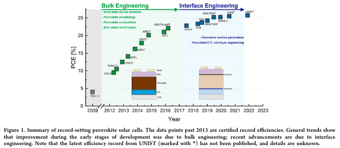
“In the early development stages of PSCs, significant progress
in PCE was realized by combining key features of innovative
device configurations (including sensitized, mesoscopic, and
planar heterojunction structures), film deposition methods
(including one-step and two-step sequential deposition), and
chemical composition engineering (including of materials such
as methylammonium (MA), formamidinium (FA), double and
triple cations, and mixed halides) of perovskite material” (Yoo et al., 2022, p. 1) MA: Methylam monium
FA: Formamidinium
“Organic ammonium halides
have been explored as surface passivators to modify the
perovskite surface or to generate 2D perovskites on top of 3D
perovskites, resulting in an effective reduction in surface defect
density and large increases in open-circuit voltage (VOC)” (Yoo et al., 2022, p. 1) passivation strategy:
Adding Organic ammonium halides to make 2D perovskite on the top of 3D perovskite.
It improves Voc and FF
“Furthermore, these passivation layers can
provide a hydrophobic nature to the perovskite surface and
effectively inhibit ion migration, resulting in remarkably
improved stability.” (Yoo et al., 2022, p. 2) The effect of passivation layer:
- Provide hydrophobic nature
- Inhibit ion migration
—> therefore, a better stability
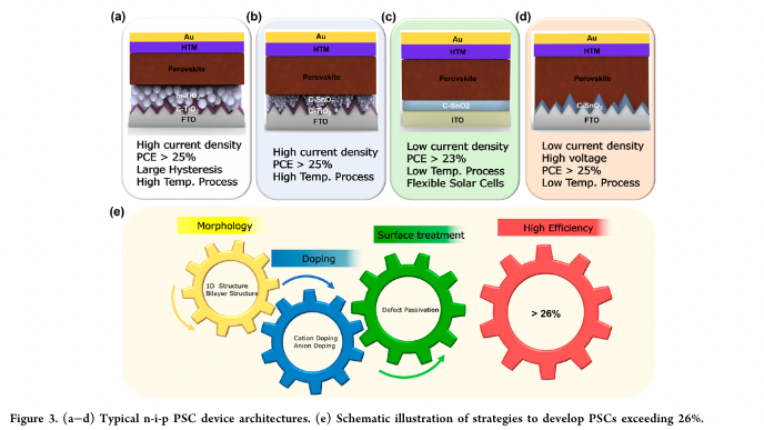
“shows the conventional n-i-p architecture for PSCs consisting of four different electron-transport structures. The mesoscopic n-i-p is the original PSC structure that is still” (Yoo et al., 2022, p. 3)
“widely used to fabricate high-performance PSCs (Figure 3a).15,27” (Yoo et al., 2022, p. 4)
“mesoscopic PSC is generally composed of dense
anatase TiO2 and mesoscopic anatase TiO2 nanoparticles
(NPs), which are crystallized by high-temperature processing
at over 450 °C. Such high temperature improves the
crystallinity and forms necking among each NP, which
improves the electron-transport properties of the film. It was
recently reported that lithium-doped mesoscopic TiO2, in the
form of lithium carbonate, can further improve the electrical
properties of mesoporous TiO2, which can result in high
current density of over 26 mA/cm2, thereby achieving device
efficiency exceeding 25%.34 However, the mesoscopic TiO2
structure remains problematic for large-scale production.” (Yoo et al., 2022, p. 4) Mesoscopic PSC:
- Dense anatase TiO2/mesoscopic anatase Ti02 nano particle.
- Crystallized at 450 C -> improve the electron transport properties.
- doped with Lithium carbonate further improve the electrical properties
- Difficult to large-scale production
“Generally, TiO2 possesses oxygen vacancies or surface
defects” (Yoo et al., 2022, p. 4) TiO2 possesses oxygen vacancies or surface defects.
- under voltage scan, the O vacancies acculumate in TiO2/perovskite interface. Slow the electron extraction -> cause anomalous hysteresis.
“Moreover, due to its photocatalytic properties, mesoscopic TiO2 can degrade the perovskite layer under light illumination; this leads to poor long-term photostability, which can hinder commercialization of PSCs.” (Yoo et al., 2022, p. 4)
“Among the alternatives to TiO2, Sn-based metal oxides have
been found to be the best alternative for PSCs because their
conduction band minimum (CBM) primarily originates from
the Sn 5s-O 2p orbital interaction, giving rise to a large CB
dispersion with low effective mass, where lower effective mass
results in higher electron mobility.” (Yoo et al., 2022, p. 4) They use BaSnO3 or SnO2.
- non-photocatalystic properties. ?? How this photocatalystic works. Why degrading the perovskite?
“This structure (SnO2 QDs/dense TiO2) enables an impressive device performance, beyond 25%, without hysteresis, along with a value of JSC exceeding 26 mA/ cm2, all of which make this material comparable to the best mesoscopic TiO2-based PSCs.” (Yoo et al., 2022, p. 4)
“Unfortunately, to fully cover the rough FTO surface with dense TiO2, this structure still uses a spray pyrolysis technique that requires a sintering temperature of 450 °C. A” (Yoo et al., 2022, p. 4)
“One way to decrease the processing temperature to 100 °C is to use crystalline colloidal NPs with particle size below 5 nm.” (Yoo et al., 2022, p. 4)
“However, when SnO2 NPs only are used on ITO, the current density is much lower when compared to that obtained using high-temperature-processed PSCs. To solve this problem, a bilayer structure composed of porous films using Zn2SnO4 NPs of 20 nm in particle size and dense SnO2 NP films has been proposed.” (Yoo et al., 2022, p. 4)
“As an
alternative, the chemical bath deposition (CBD) method for
uniformly forming a thin film of SnO2 on the FTO surface was
developed (Figure 3d).19 Thin films produced using CBD have
significantly higher packing densities, without pinholes, when
compared to existing films formed using colloidal SnO2 NPs.” (Yoo et al., 2022, p. 4) To make th SnO2 layer more uniform
“To completely cover the FTO or ITO substrate with only
NPs, the NP film must be deposited thickly enough to
overcome the low NP packing density. However, because the
diffusion length of the NP film is short, thick films cause large
reductions in electron-transport properties.41 Therefore, the
key to achieving high-efficiency PSCs is to improve the
electrical properties of the NP film itself.” (Yoo et al., 2022, p. 4) - To cover the ITO or FTO completely, the Nanoparticle should be thick enough
- But too thick will give bad electron transport properties. The diffusion length is short.
- Need additional doping to improve the electrical properties.
“the employment of low-vapor-pressure solvents that can coordinate with PbI2, such as DMSO and NMP, which can stabilize the PbI2-complex intermediate phase, retard nuclea- tion, and allow controlled growth of the perovskite poly- crystals. Later, using various additives such as alkali metals, Lewis acids/bases, and large organic cations, researchers began improving the phase stability of the α-FAPbI3 perovskite, which is also referred to as the “black phase” because it has a much narrower bandgap than the “yellow” δ-FAPbI3 phase.13,14,27,46-48” (Yoo et al., 2022, p. 5)
“For example, the addition of alkali metals (e.g., Cs, Rb, etc.) with smaller ionic radii leads to more ideal Goldschmidt tolerance factor, and this results in perovskite compositions that are more stable to external stresses and homogeneous. This effort allowed researchers to move away from MAPbI3-based perovskite, which exhibited poor thermal and moisture stability in long-term studies.” (Yoo et al., 2022, p. 5)
“As the surface (or the interface with the CTL) is susceptible to defects and interface recombination, a wide library of passivation strategies were developed. To date, the most popular method to manage surface-related defects is to deposit a wide-bandgap material (either by forming a wide- bandgap quasi-2D perovskite in situ, or via a molecular approach) on the exposed surface.” (Yoo et al., 2022, p. 5)
“To passivate the surface of perovskite thin films and characterize the bulk properties, deposition of a thin layer of TOPO has become a popular method because it allows researchers to decouple contributions from the surface from those of the bulk.49” (Yoo et al., 2022, p. 5)
“To solve the problem of inefficient absorption near the band edge, a strategy to increase the thickness of the polycrystalline perovskite photo- active layer while maintaining low surface roughness and avoiding neg- ative effects on the carrier transport properties needs to be developed.” (Yoo et al., 2022, p. 6)
“On the other hand, most efficient PSCs employ Spiro- OMeTAD as a hole-transport layer (HTL). However, it does not ensure device reliability and long-term stability under a damp-heat condition.” (Yoo et al., 2022, p. 7)