Printable Low-Temperature Carbon for Highly Efficient and Stable Mesoscopic Perovskite Solar Cells
(2022) - Nivethaa Ravi Thangavel, Teck Ming Koh, Zhong Quan Chee, Darrell Jun Jie Tay, Ming Jun Lee, Subodh G. Mhaisalkar, Joel W. Ager, Nripan Mathews
- Link:
- DOI: 10.1002/ente.202200559
- Zotero Link: Printable Low-Temperature Carbon for Highly Efficient and Stable Mesoscopic Perovskite Solar Cells
- Tags: #paper
- Cite Key: [@thangavelPrintableLowTemperature2022]
- Linked notes: Paper Annotations
Abstract
Figures
Notes
Annotations (3/10/2023, 5:22:11 PM)
“Interestingly, the work function of carbon (5.1 eV) is close to that of gold metal (5.0 eV) which allows it to be an alternative material for the rear electrode.[6]” (Thangavel et al., 2022, p. 1) #nodes_research the work function of carbon is (5.1 eV) almost the same as gold (5.0)
“This fully printable architecture, which usually consists of triple mesoporous layers of TiO2 as the electron transporting layer, ZrO2 or Al2O3 as the spacing layer, and carbon as the counter electrode, can be realized through a cost-effective” (Thangavel et al., 2022, p. 1) alternative to Zr02,we can use Al2O3
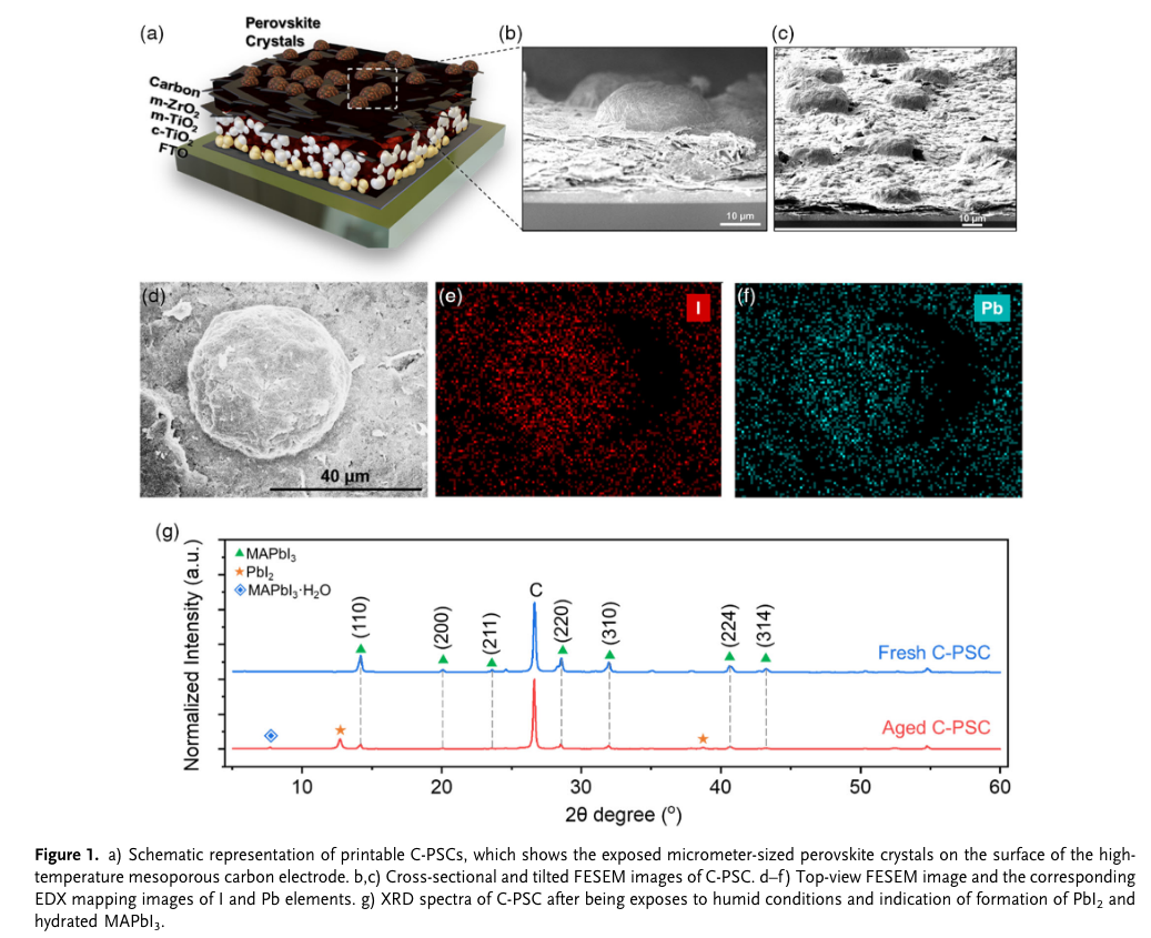
“The proper filling of perovskite solution in the mesoporous scaffold is strongly governed by many factors, such as the volume of perovskite solution, surface wetting, droplet size, and droplet location.[6,7] Any unoptimized infiltration process would easily lead to C-PSCs with poor reproducibility. However, even though a proper perovskite infiltration was done, there is another unavoidable issue in C-PSCs, which is the formation of nonfunctional perovskite crystals on mesoporous stacks from the excessive solution that stays on the device scaffold.” (Thangavel et al., 2022, p. 2) why infiltration is affected by perovskite solution, surface wetting, droplet size, droplet location.
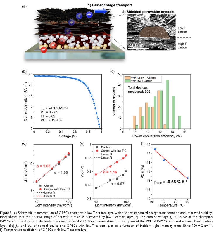
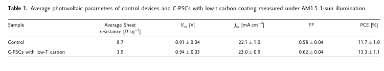
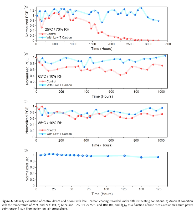
“We demonstrate the application of the additional printable low-temperature (low-T)-processed highly conductive carbon layer to improve the device stability and enhance the charge conduction and the overall photovoltaic performance. The C-PSCs with low-T carbon coating display an improved power conversion efficiency of 15.4% with a major enhancement from fill factor (FF) and open-circuit voltage (Voc). The device with low-T carbon coating shows great advancement in moisture stability over 3,250 h under 70% relative humidity (RH) as compared with the control device and stable device output at 65 and 85 °C over 1,000 h without any physical encapsulation.” (Thangavel et al., 2022, p. 2)
“Once the perovskite material is hydrated, it will transform into methylamine and hydroiodic acid (HI) which will undergo further degradation in the presence of oxygen through a cyclic chemical reaction.” (Thangavel et al., 2022, p. 2) #nodes_research when perovskite exposed to open air, or hydrated, it will transform intomethylamine and hydroiodic acid (HI). Then udergo further degradataion in the presence of oxygen through a cyclic chemical reaction.
“The presence of excess PbI2 upon moisture degradation can be easily observed as a yellow decomposition product at or around the active area of perovskite solar cells” (Thangavel et al., 2022, p. 2) #nodes_research what is the yellow part? it is a decomposition product of PbI2 upon moisture degradation
“X-Ray diffraction analysis (XRD) was performed on fresh and aged (kept 1 month under 70% RH) C-PSCs (Figure 1g). The XRD pattern in the freshly fabricated device indicates the characteristic peaks at 14.2°, 20.1°, 23.6°, 28.6°, 32.0°, 40.6°, and 43.2° corresponding to the (110), (200), (211), (220), (310), (224), and (314) lattice planes of MAPbI3.[11] Nevertheless, upon exposing the device to humidity, a hydrated perovskite phase is detected at around 7.7° along with the weak perovskite peak and the emergence of the PbI2 characteristic peak at 12.7°, indicating the degraded perovskite in C-PSCs.[12]” (Thangavel et al., 2022, p. 2) #nodes_research
the degraded perovskite can be seen from XRD
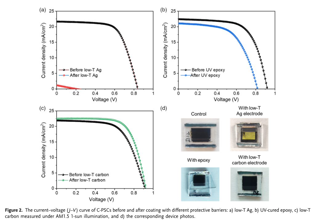
“It has been shown that the combination of Ag electrode and perovskite could lead to a chemical reaction and resulted in the formation of several decomposition byproducts including silver iodide and lead iodide.[13]” (Thangavel et al., 2022, p. 2) #nodes_research
the interaction of Ag and perovskite can lead to a formation of several decomposition byprodcts including silver iodide and lead iodide.
“In general, Voc loss in PSCs is associated with the energy alignment and recombination, and we expect the same to be true in C-PSCs. The dependence of Voc on light intensity can be used for the analysis of trap-assisted recombination. It is a well-known accepted fact in the solar cell community the trap-assisted recombination dominates the recombination mechanism in PSCs and limits their efficiency. Grain boundaries and interfaces become the primary location for trap-assisted recombination. The ideality factor (nid), which is obtained from the plot of Voc versus light intensity, demonstrates the dominating type of recombination. The ideality factor is obtained from the following equation. ηid ¼ q kB T dVoc dðlnðIÞÞ (1)” (Thangavel et al., 2022, p. 4) #nodes_research how to correlate Voc and recombination by analyzing the dependency of Voc with light intensity
“If nid > 1, Shockley–Read–Hall (SRH) recombination is said to dominate, and if nid ¼ 1, bimolecular recombination is said to dominate. If the ideality factor is close to 1 kT/q, it indicates that the device is good with low bulk” (Thangavel et al., 2022, p. 4)
“recombination and very good interfaces.” (Thangavel et al., 2022, p. 5)
“Materials: Blocking layer TiO2 paste (BL-1), meso-TiO2 paste (30 NR-D), methylammonium iodide (MAI), and 5-ammonium valeric acid iodide (5-AVAI) were purchased from Greatcell Solar. The meso-TiO2 paste was diluted with Terpineol (SigmaAldrich) in a ratio of 1:1.4 for screen printing. TiCl4 was purchased from FUJIFILM Wako Pure Chemical Corporation. ZrO2 paste (Zr-Nanoxide ZT/SP) was purchased from Solaronix. High-temperature carbon paste was purchased from Hubei Wonder Solar LLC. Low-T carbon paste was purchased from Guangzhou Seaside Technology Co., Ltd. Lead iodide (PbI2) (99.99%, trace metal basis) and γ-butyrolactone (GBL, 99.0%) were purchased from Tokyo Chemical Industry. Methylammonium chloride (MACl) was purchased from Merck Millipore Corporation. Perovskite Solution Preparation: All the chemicals were used without further purification, except GBL. GBL was dried with molecular sieves which were heated in an oven at 400 °C for 4 h. The perovskite solution was prepared inside an Ar-filled glovebox, and the oxygen and moisture levels were kept at 0.1 ppm. To prepare the AVAxMA(1 x) PbI3 composition, 1.2 mole of PbI2, 1.2 mole of MAI, 0.45 mole of 5-AVAI, and 0.1 mole of MACl were added in 1 mL of GBL. The final solution was stirred and heated at 50 °C until a clear solution was obtained. Device Fabrication: Patterned FTO substrates were cleaned in an ultrasonicator thrice with decon soap solution, followed by deionized (DI) water and ethanol. Each sonication step took place for 30 min. After sonication, the substrates were dried and treated by UV–ozone for 20 min. The compact TiO2 layer was screen printed using a screen printer (MicroTec MT320TV) on the cleaned substrate, and it was annealed at 500 °C for 30 min with 40 min ramping rate. Subsequently, a 500 nm-thick mesoporous TiO2 was screen printed and annealed at 500 °C for 30 min with 40 min ramping rate. Next, the substrate with meso-TiO2 was dipped into TiCl4 solution (2 mL of TiCl4 in 100 mL of DI water) and left at 70 °C for 30 min in an oven. The dried substrates were then annealed at 500 °C for 30 min with 40 min ramping rate. Next, 1 𝜇mthick mesoporous ZrO2 was screen printed and annealed at 500 °C for 30 min with 40 min ramping rate. Finally, high-temperature mesoporous carbon electrode was screen printed and annealed at 400 °C for 30 min with 30 min ramping rate. For perovskite infiltration, 4 𝜇L of perovskite solution was drop cast onto a 0.7 cm2 mesoporous scaffold and sequential annealing process took place at 50 °C for 90 min and followed by at 100 °C for 60 min to complete the crystallization. The entire process of perovskite infiltration and the annealing process were conducted in a controlled environment where the relative humidity was maintained at 40%. The infiltrated devices were different materials to shield the exposed perovskite crystals. All the processes except infiltration and annealing of perovskite took place in ambient laboratory atmosphere.” (Thangavel et al., 2022, p. 7) #nodes_research Carbon perovskite fabrication method
“Coating methods of these materials were as follows: low-T Ag paste and low-T carbon paste were screen printed over the infiltrated C-PSCs and annealed at 120 °C for 30 min at the ramp rate of 5 min. UV-curable epoxy was carefully applied over the active region of the infiltrated carbon device in the nitrogen-filled glove box and cured for 18 s under UV illumination.” (Thangavel et al., 2022, p. 8) how to print Ag. anneal it 120 C for 30 min at ramp rate 5 min.
Nripan's group