Halide Perovskites for Memristive Data Storage and Artificial Synapses
(2021) - Kyung Ju Kwak, Da Eun Lee, Seung Ju Kim, Ho Won Jang
- Link:
- DOI: 10.1021/acs.jpclett.1c02332
- Zotero Link: Halide Perovskites for Memristive Data Storage and Artificial Synapses
- Tags: #paper
- Cite Key: [@kwakHalidePerovskitesMemristive2021]
- Linked notes: Paper Annotations
Abstract
Halide perovskites have been noted for their exotic properties such as fast ion migration, tunable composition, facile synthetic routes, and flexibility in addition to large light absorption coefficients, long carrier diffusion lengths, and high defect tolerance. These properties have made halide perovskites promising materials for memristors. Applications in the field of resistive switching memory devices and artificial synapses for neuromorphic computing are especially noteworthy. This Perspective covers state-of-the-art perovskite-based memristive devices. Moreover, the fundamental mechanisms and characteristics of perovskite-based memristors are elucidated. Interesting opportunities to improve the performance of perovskitebased memristors for commercialization are provided, including improving film uniformity and air stability, controlling the stoichiometry, finding new all-inorganic and lead-free halide perovskites, and making perovskites into single crystals or quantum dots. We expect our Perspective to be the foundation of realizing next-generation halide perovskite-based memristors.
Notes
Annotations (9/26/2022, 8:53:04 AM)
“Artificial synapses represent a promising concept for new memory because, in the case of crossbar arrays, in-memory computing can be realized.1” (Kwak et al., 2021, p. 1)
“resistive switching memory (RSM)” (Kwak et al., 2021, p. 1)
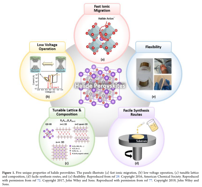
“On the other hand, for halide perovskites, there is a soft bonding between metal and halide ions, which facilitates the movement of ions.” (Kwak et al., 2021, p. 1)
“Because halogen anions have a soft bonding with metal, they can facilitate the movement of ions.” (Kwak et al., 2021, p. 2)
“The formation energies of intrinsic point defects in halide perovskites in both organic and inorganic halide perovskites have been reported to be low.7,8 Moreover, the defect concentration in halide perovskites can be adjusted by controlling the mixing ratio of each element in the precursor,9 which means it is easy to control ion migration in halide perovskite-based memristors (Figure 1a)” (Kwak et al., 2021, p. 2)
“Furthermore, it is easy to tune the lattice and the composition of halide perovskites through changing types and ratio of each element.” (Kwak et al., 2021, p. 2)
“To date, halide perovskites have relatively poor environmental stability (lasting for only a few days),11 and this can be enhanced by dimension engineering. 2D perovskites, which have general formula R2An-1BnX3n+1, where R is a bulky organic cation such as an aliphatic or aromatic alkylammonium that is used for a spacer between each layer and n is the number of halide perovskite layers between bulky organic cations,” (Kwak et al., 2021, p. 2)
“Because the memristor does not just judge the existence of the charge but also recognizes the magnitude of the resistance, memristors open the possibility of more complex data storage era compared with conventional CMOS memory devices.” (Kwak et al., 2021, p. 3)
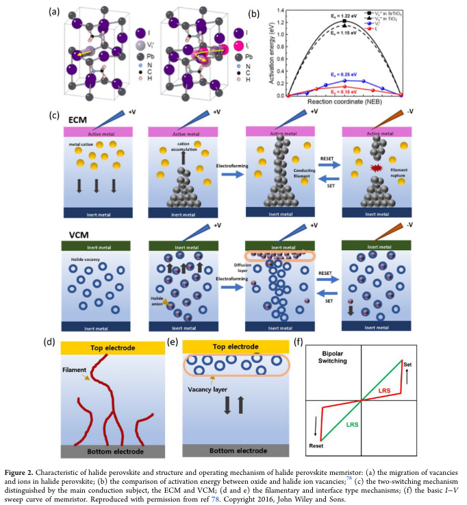
“The change in resistance can be explained by two types of mechanisms according to the type of conducting path. One is called electrochemical metallization mechanism (ECM), and the other is called valence change mechanism (VCM).” (Kwak et al., 2021, p. 3)
“ECM refers to the resistance change caused by the formation and rupture of metal cation filaments by an active metal electrode (e.g., Ag and Cu).” (Kwak et al., 2021, p. 3)
“On the other hand, the VCM refers to resistance change caused by vacancy when inert metals are used as electrodes.” (Kwak et al., 2021, p. 3)
“When the external bias is applied, metal cations are repulsed toward the bottom electrode, and accumulation of these cations leads to conductive filaments in a semiconductor layer in the ECM while the ions, which are usually halide anions or oxide anions, are attracted toward a top electrode, making a diffusion layer between the semi- conducting layer and inert metal and a conducting path consisting of vacancies in the VCM. I” (Kwak et al., 2021, p. 3)
“In halide perovskite-based memristors, the conducting path consists of either metal cations for the ECM or halide vacancies for the VCM, which is quite similar to conventional oxide-based memristors” (Kwak et al., 2021, p. 3)
“When the opposite bias is applied, the RESET process occurs. The conducting paths break down because of the movement of cations or ions, leading the semiconducting layer to turn into a high-resistance state (HRS), which is called the OFF state. The breakdown of the conducting filament does not mean the complete return of cations or ions to the initial place. Instead, the conduction paths are partially broken. Therefore, after the first RESET process, turning the HRS to LRS requires less power compared to the electroforming process. This is called the SET process.” (Kwak et al., 2021, p. 3)
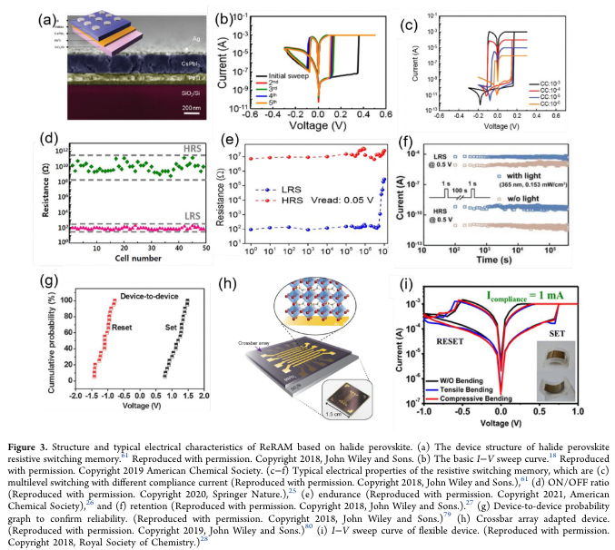
“Two types of memories are required to meet the needs of industry, which are DRAM, a volatile memory but with high speed, and NAND flash, a nonvolatile memory but with low speed. To overcome these obstacles, researchers suggest new types of memories. Above all, resistive switching memory (ReRAM) is getting a great deal of attention because of its fast speed, low power consumption, extremely small cell, and high endurance.” (Kwak et al., 2021, p. 4)
“There are several parameters to be measured to evaluate the performance of the device. The first index is I-V character- istics. The hysteresis and operating voltage can be confirmed by the I-V curve. The operating voltage indicates the voltage that causes ReRAM to the opposite resistance state. ON voltage means the voltage when the HRS turns into LRS, and OFF voltage means the voltage when the HRS turns into LRS.
Lower operating voltage means lower power consumption” (Kwak et al., 2021, p. 4)
“The second one is the ON/OFF ratio.” (Kwak et al., 2021, p. 5)
“Considering the conventional flash memory, this figure should reach more than 1010.” (Kwak et al., 2021, p. 5)
“For the perovskite-based ReRAM, 109 is the best value to date” (Kwak et al., 2021, p. 5)
“The third value is endurance. It refers to the maximum number of reversible cycles that the device can stably change between HRS and LRS.” (Kwak et al., 2021, p. 5)
“Flash memories that are commercially available have endurance cycles between 103 and 107.” (Kwak et al., 2021, p. 5)
“The value of 6 × 10³ is the best to date for halide perovskites. Poddar et al. fabricated a Ag,ITO/MAPbI3 quantum wire in a PAM/CsPbBr3 QDs/PMMA/Au/PET substrate device. The reversible cycle number was found to be up to 6 × 10³, which is provided in Figure 3e.
26” (Kwak et al., 2021, p. 6)
“The fourth value is retention. It refers to how long the data can be stored in the device.” (Kwak et al., 2021, p. 6)
“The experimental data is obtained by applying voltage to make the device to LRS or HRS and reading the resistance with an extra small voltage.” (Kwak et al., 2021, p. 6)
“More than 105 s of endurance is reported for Wang et al.'s device with the structure of Ag/PMMA/CsPbBr3 QDs/ PMMA/ITO, which can be seen in Figure 3f.27” (Kwak et al., 2021, p. 6)
“The last value is switching speed. By measuring the width of write voltage pulses which can change the resistance state o” (Kwak et al., 2021, p. 6)
“In the most widely used memory, the DRAM and NAND flash each have the switching speed of 10 ns and 10 ms, respectively” (Kwak et al., 2021, p. 6)
“Hwang et al. fabricated the Au/(CH3NH3)3Bi2I9(MABI)/ITO ReRAM, which showed ultrafast switching speed of 100 ns.28” (Kwak et al., 2021, p. 6)
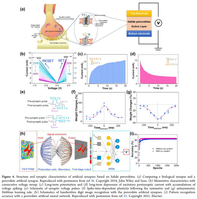
“In biological nervous systems, a general neuron is composed of the soma, dendrite, and axon. They connect with each other to conduct various functions at the network level, such as recognition, processing, and memo- rization. Numerous neurons are linked via the synaptic junction, called synapses, which transmit signals chemically (chemical synapses) or electrically (electrical synapses). A typical human brain consists of about 100 billion neurons30 and 500 trillion synapses.31 The chemical synapse consists of pre- and postsynaptic membranes and a synaptic cleft. The axon terminal of the presynaptic neuron attaches to the dendrite of postsynaptic neurons. When the action potential reaches the axon terminal, it causes voltage-gated calcium channels to open and induces the vesicles containing neurotransmitters to fuse with the membrane. The neuro- transmitters are released from the presynaptic membrane to the postsynaptic membrane for transmitting chemical signals to action potentials. Through this neuron facilitation, the synapses can modulate their strength of connecting adjacent” (Kwak et al., 2021, p. 7)
“neurons by excitation and inhibition. This characteristic is called synaptic plasticity.” (Kwak et al., 2021, p. 7)
“In 2016, Huang et al. first reported MAPbI3-based artificial synapses.32” (Kwak et al., 2021, p. 7)
“diverse halide perovskite materials, such as MAP- bI3-xClx, 33 PEA2PbBr4, 34 MAPbBr3, 35,36 FAPbBr3, 36,37 CsPbBr 3 , 3 6 PEA2MAn-1PbnB r 3 n + 1 , 3 8 (Cs 3Bi 2 I 9 ) 0.4 - (CsPbI3)0.6, 19 MA3Sb2Br9, 39 Cs3Cu2X5, 40 Cs2AgBiBr6, 41 and CsPbI2Br,42 were explored to demonstrate artificial synaptic devices.” (Kwak et al., 2021, p. 7)
“Very recently, Yang et al. reported the two-terminal Ag/ P3HT/CsPbBr2I/ITO artificial synapses to implement self- powered artificial retina systems.43” (Kwak et al., 2021, p. 7)
“They reported a halide perovskite memristor with P3HT layer between Ag top electrode and perovskite layer. This passivation layer can protect Ag penetration from perovskite films, enhancing memristive properties and ambient air stability” (Kwak et al., 2021, p. 7)
“Figure 4c,d presents a long-term potentiation and depression process of excitatory postsynaptic current (EPSC) with the accumulation of voltage spiking. The gradual EPSC increase, which is called potentiation, occurred when the 100 times repeated positive voltage pulses were applied (magni- tude, 0.4 V; width, 100 ms; interval, 100 ms). In dontrast, the gradual EPSC decrease, which is called depression, occurred when the 100 times repeated negative voltage pulses were applied (magnitude, -0.4 V; width, 100 ms; interval, 100 ms).” (Kwak et al., 2021, p. 7)
“Furthermore, they demonstrated the spike-time-dependent plasticity (STDP) in their perovskite artificial synapses. In biological neural systems, the neurons process the signal information by adjusting their synaptic connection strength” (Kwak et al., 2021, p. 7)
“depending on the time difference between presynaptic and postsynaptic neuron activation. This behavior is regarded as the Hebbian learning rule. To achieve symmetric and antisymmetric Hebbian learning rules, the presynaptic spike (0.7 V, 1 s or -0.7 V, 1 s) and postsynaptic spike (-0.3, 1, or 0.3 V, 1 s) were successively applied to the perovskite artificial synapse with a time difference, as shown in Figure 4e.” (Kwak et al., 2021, p. 8)
“Moreover, to verify the possibility of neuromorphic computing, they demonstrate the artificial retina system to perform pattern recognition with handwritten digit images (Figure 4h,i). An accuracy of 85.63% was achieved within 180 training epochs, indicating the improvement of low-voltage operation computing with perovskite artificial synapses.” (Kwak et al., 2021, p. 8)
“In particular, the typical three-dimensional halide perovskite of MAPbI3 is well-known to degrade into PbI2 when exposed to high-temperature and humid conditions.44,45” (Kwak et al., 2021, p. 8)
“For example, the large organic A-site cations form the two- dimensional halide perovskites, which stabilize with layered perovskite structures. The bulky organic cations contribute as a steric stabilizer and the shielding spacer for surface water adsorption.46,47 Thus, they enhanced the thermal and moisture stability compared to the 3D perovskites.” (Kwak et al., 2021, p. 8)
“The double perovskites have two different metallic B-site cations that form the same average charge of the existing B-site cation in ABX3. These crystal structures which have two different B- site metal cations enhance the air stability.48,49 Recently, dual- phase halide perovskite memristors were reported to increase the phase stability and memristive performance.19,50” (Kwak et al., 2021, p. 8)
“Stoichiometry. Especially in the layer-structured 2D and quasi
2D halide perovskites, the bulky organic cations confine the
charge carriers within layered perovskite sheets. These
alternating formations of large organic interlayers and
inorganic perovskite sheets form the multiple-quantum-well
structure. Their dielectric contrast induces a huge electron-
hole binding energy in their layered perovskites. Compared to
the 3D perovskites, this layered structure typically induces a
large exciton binding energy of about 0.1 eV, which
significantly promotes the electrical interaction between
electrons and holes. Because of this band structure and large
binding energy, the low number of perovskite layers in 2D
perovskites (n = 1-5) often show a high barrier of charge
transport across the adjacent inorganic perovskite layers. In
general, n = 1 represents the pure 2D perovskites, and until n =
5 is often known as quasi-2D perovskites. The n value of such
perovskites is usually described based on the precursor
composition.” (Kwak et al., 2021, p. 8) Why 2D perovskite good for passivation
“Especially for the case of methylammonium lead iodide, it is intrinsically unstable because the decomposition reaction of methylammonium lead iodide, MAPbI3 → MAI + PbI2, is exothermic and can occur without external stimuli.57” (Kwak et al., 2021, p. 8)
“Inorganic halide perovskites are expected to show better stability by eliminating the weakly bonded organic elements.58” (Kwak et al., 2021, p. 8)
“When methylammonium is replaced by cesium,” (Kwak et al., 2021, p. 8)
“the vibrational entropy can improve the stability of the structure of halide perovskites, and because Cs cation is free of acid protons, it can be more oxygen-tolerant under light.59” (Kwak et al., 2021, p. 9)
“Cesium-based all-inorganic halide perovskites are being actively studied.60-64” (Kwak et al., 2021, p. 9)
“Tin was one of the first elements suggested to substitute lead because tin is easily turned into a divalent cation state so that tin-based halide perovskites have the same stoichiometry with lead-based halide perovskites.” (Kwak et al., 2021, p. 9)
“Pt, ITO)/poly(methyl methacrylate) (PMMA)/CsSnI3/top electrode (Au, Ag)18 was successfully fabricated and showed good resistive switching behavior. However, tin is easily oxidized into Sn4+ because of the higher energy level in the 5s orbit. It means that Sn-based halide perovskites are vulnerable to air and water” (Kwak et al., 2021, p. 9)
“Therefore, a trivalent metal cation such as Bi3+ and Sb3+ is adapted as a substituent. Memristors with a structure of Al/CsBi3I10/ITO,71 PET/ITO/Cs3Bi2I9/Au,72 and ITO/(MA)3Bi2I9/Au28 showed excellent stability. H” (Kwak et al., 2021, p. 9)
“However, because electrical conduction of the low-dimensional structure is not good, these memristors required higher operating voltage compared with lead-based devices” (Kwak et al., 2021, p. 9)
“The most currently studied halide perovskite is the double perovskite. Two lead sites are substituted by two metal cations, one monovalent cation and one trivalent ion. Their stoichiometry is A2M1 +M2 3+X6. ITO/Cs2AgBiBr6/Au73 was fabricated and showed not only good stability but also low power consumption.” (Kwak et al., 2021, p. 9)
“Considering the tunability of the lattice and composition of halide perovskite, discovering new nonlead-based halide perovskites is limitless.” (Kwak et al., 2021, p. 9)
moved to Zotero