Effect of Excess PbI2 in Fully Printable Carbon-based Perovskite Solar Cells
(2017) - Vishakha Kapoor, Amna Bashir, Lew J. Haur, Annalisa Bruno, Sudhanshu Shukla, Anish Priyadarshi, Nripan Mathews, Subodh Mhaisalkar
- Link:
- DOI: 10.1002/ente.201700484
- Zotero Link: Effect of Excess PbI2 in Fully Printable Carbon-based Perovskite Solar Cells
- Tags: #paper
- Cite Key: [@kapoorEffectExcessPbI22017]
- Linked notes: Paper Annotations
Abstract
Excess lead iodide (PbI2) has been reported to improve the power conversion efficiency (PCE) in the standard perovskite solar cell (PSC) with 2,2,7,7-Tetrakis(N,N-di-p-methoxyphenyl-amine)-9,9- spirobifluorene (spiro-OMeTAD) as a hole-transporting material. In this study, we studied the effect of having excess PbI2 in fully printable carbon-based perovskite solar cells (PSC). Excess amounts of PbI2, ranging from 0 % to 15 %, were added to the equimolar perovskite solution for infiltration in the carbon-based PSC architecture. There was an improvement in the average value of open-circuit voltage (0.87 to 0.91 V) with increased PbI2, but there was no clear trend in fill factor and current density. All devices showed good stability under ambient conditions without encapsulation. The device containing 15 % excess PbI2 showed degradation under continuous illumination, whereas there was no degradation with an equimolar ratio of perovskite precursors.
Notes
Annotations (1/3/2023, 10:44:48 AM)
“Asmallamount ofexces sPb2 I intheperovskite layer has been demonstrated toimprovethepower conversion efficiencies ofdevices across variousperovskitesinthestanda rd device architecture.[8]” (Kapoor et al., 2017, p. 1880)
“Reduced recombinationhasbeen observed insamples containingasmall amount ofexcess PbI2.[8d,9] Ithasbeen suggested that PbI2 hasapassivation effect between thecrystal grains oftheperov skite,[8c,9a] and attheinterfac ebetweentheperov skite andTiO 2,therebyresultinginlower recombination rates.[8d,10] Excess PbI2 inthe precursorsoluti onalso appearstoincreast ehesize ofthe perovskite grains forme” (Kapoor et al., 2017, p. 1880)
“ed.[8a,d]” (Kapoor et al., 2017, p. 1880)
“Inthis work, weinvesti gate theeffects ofexces sPbI 2 in fully printable carbon-based devices.Thecrystal phase composition and light absorption oftheperov skite film with excess PbI2 werecomprehens ively examined byX-raydiffer ential detection (XRD),UV/V isabsorp tion spectra, andphotoluminescence(PL)spectra. Time-resolved photoluminescence (TRPL) decay was used tounderstand thecharge transportmechanism .Finally ,thestability ofthese devices under ambient conditions(25 8Cand65%RH)and under continuousilluminat ionisdiscussed.” (Kapoor et al., 2017, p. 1881)
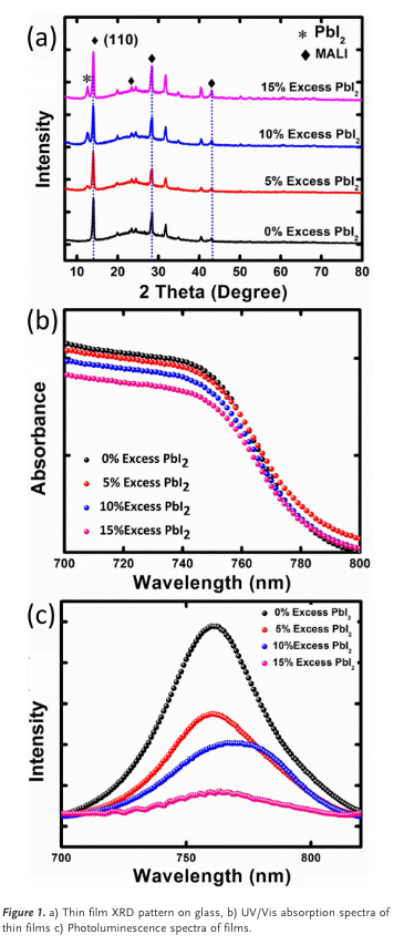
“The XRD pattern confirms the presence of the tetragonal phase of CH3NH3PbI3 in all prepared films.
No PbI2 peak (2q&12.78) was observed for the perovskite film prepared using a stoichiometric ratio of MAI and PbI2,” (Kapoor et al., 2017, p. 2)
“An increasing peak intensity cor- responding to PbI2 starts appearing with the addition and in- crease of excess PbI2 in the precursor solution as shown in Figure 1 a.” (Kapoor et al., 2017, p. 2)
“There is also an increase in intensity of the perovskite (110) peak with increased PbI2, but this effect was very slight for this set of samples, compared with those reported pre- viously.[8a” (Kapoor et al., 2017, p. 2)
“It has been posited that this effect may be caused by an observed change in grain size. To confirm this, top- view SEM was conducted for these perovskite films, as shown in Figure S1 (Supporting Information). No significant difference in grain size was observed as the PbI2 in the per- ovskite solution increased.” (Kapoor et al., 2017, p. 2)
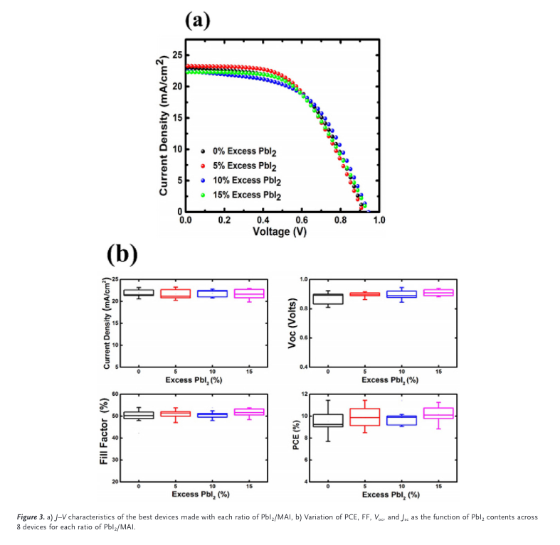
“It must be noted that the overall performance of these devices did not vary to a great degree even between the extremes of 0% and 15% excess” (Kapoor et al., 2017, p. 3)
“As the excess PbI2 content increased from 5% to 10%, the Voc increased from 0.92 V to 0.94 V, and it remained at approximately 0.94 V with 15% excess. The Jsc, however, de- creased (by less than 5% of the maximum) as the excess PbI2 content was increased beyond 5%, and the FF remained at approximately 53.8% for all devices, thereby resulting in similar PCEs from the best devices of each value of PbI2 con- tent.” (Kapoor et al., 2017, p. 3)
“The average Voc for each value appears to increase with excess PbI2, moving from 0.87 V without excess PbI2 to 0.91 V with 15% excess PbI2, which is consistent with previous studies.
[8a–e]” (Kapoor et al., 2017, p. 3)
“Although previous reports have generally agreed that excess PbI2 in the perovskite layer improves the device efficiency, they are not wholly consistent on the optimal amount of PbI2 necessary to achieve this effect, or on the precise impacts of excess PbI2 on the Voc, Jsc, and FF. This is possibly due to differences in the processing conditions. The excess PbI2 may be distributed within the perovskite grains,[8f] at the grain boundaries,[9a,13] or at the perovskite/” (Kapoor et al., 2017, p. 3)
“TiO2 interface,[8c,10] to varying degrees depending on the dep- osition process and sintering conditions.” (Kapoor et al., 2017, p. 4)
“XRD measurements were performed on complete devices, as shown in Figure S2 (Supporting Information). The XRD data from devices is consistent with the data obtained from perov- skite films deposited on glass.” (Kapoor et al., 2017, p. 4)
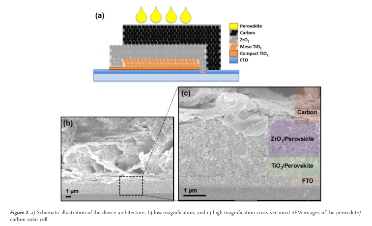
“The cross-sectional SEM images of devices contain- ing 0% and 15% excess PbI2 are presented” (Kapoor et al., 2017, p. 4)
“Previous reports have noted a difference in morphology of the perov- skite in the mesoporous TiO2 layer.[8a] In the samples pre- sented here, there is no visible difference in the mesoporous” (Kapoor et al., 2017, p. 4)
“This could indicate that excess PbI2 does not cause a stark difference in morphology of the perovskite in this porous system, or it could signify that the excess PbI2 does not reach the TiO2 and ZrO2 layers by the infiltration method and solvent used, considering the low solubility of PbI2 in gamma-butyrolactone (GBL).[” (Kapoor et al., 2017, p. 5)
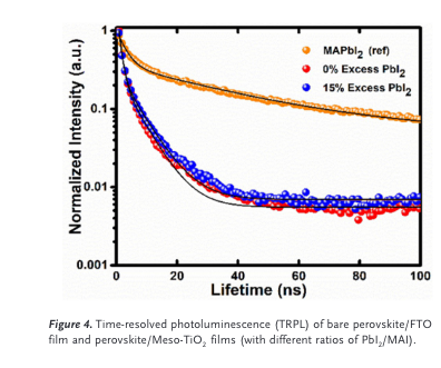
“To study the effect of excess PbI2 on the perovskite/TiO2 interface, time-resolved photoluminescence decay (TRPL) was measured” (Kapoor et al., 2017, p. 5)
“The decay curve is fitted with bi-exponential function to obtain the relaxation lifetimes. Average decay times of 20.2, 3.4, and 3.5 ns were obtained for the reference film of perovskite, the sample of perovskite/TiO2 with 0% excess PbI2, and the sample of per- ovskite/TiO2 with 15% excess PbI2, respectively.” (Kapoor et al., 2017, p. 5)
“The results for these samples with and without excess PbI2 appear to be quite similar, suggesting that the PbI2 did not impact the charge carrier lifetimes in this system.” (Kapoor et al., 2017, p. 5)
“The use of different solvent systems [e.g., mixed solvents including dimethylsulfoxide (DMSO), N,N-di- methylformamide (DMF), and subsequent treatment with anti-solvents and solvent vapors] has been demonstrated to greatly enhance the grain growth and uniformity of perov- skite films (versus films processed with GBL),[11b, 15] and PbI2 itself shows poorer solubility in GBL than in DMF and DMSO.
[14] Reports observing an enhancement of crystal growth with excess PbI2 have used DMSO as solvent, or a mixed solvent of DMSO and DMF, and subsequent treat- ment with an anti-solvent.[8a,d] It seems plausible that the use of pure GBL might have hindered the reported beneficial ef- fects of excess PbI2 on the crystal growth of the perovskite.” (Kapoor et al., 2017, p. 5)
“This means that additional work will be necessary to reveal the influence of excess PbI2 on the formation of the crystal- line perovskite phase and charge carrier dynamics using dif- ferent solvent-based systems.” (Kapoor et al., 2017, p. 5)
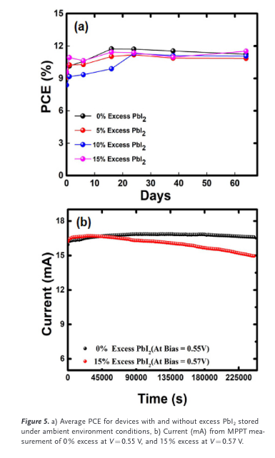
“To assess the stability of these devices, we stored them under ambient conditions (25 8C and 65% RH) without encapsula- tion, and measured the power conversion efficiency under standard AM 1.5G solar spectrum illumination at regular in- tervals for two months.” (Kapoor et al., 2017, p. 5)
“The PCEs of all devices appeared to improve over the first few days after fabrication, then remain stable for the remainder of the testing period. The initial im- provement in PCE might be due to improved crystallization of the perovskite after exposure to moisture, as has been ob- served in carbon-based PSCs.
[16]” (Kapoor et al., 2017, p. 5)
“the current reduced by ap- proximately 10% over 68 hours of continuous illumination for the device containing 15% excess PbI2.” (Kapoor et al., 2017, p. 5)
“A compositional change in PbI2 has been reported in the literature as a mechanism for this degradation.[17] Akbulatov et al. reported the formation of Pb metal or non-stoichiomet- ric Pb iodides with a composition of PbI&0.5 from the photo-degradation of PbI2.
[18]” (Kapoor et al., 2017, p. 5)
“The degradation of methylam- monium iodide under light exposure[19] and the photocatalyt-” (Kapoor et al., 2017, p. 5)
“ic activity of TiO2 [8b] are also reported to contribute to the overall degradation of the perovskite, but we see no reduc- tion in performance under continuous illumination without excess PbI2 in the carbon-based architecture over the tested time frame.” (Kapoor et al., 2017, p. 6)
“Excess PbI2 seems to im- prove the open-circuit voltage of carbon-based PSCs, but there is little benefit to other device parameters, and the overall performance in the carbon-based structure does not change.” (Kapoor et al., 2017, p. 6)
“The excess PbI2 in the fabricated devices appears to hasten degradation in this otherwise stable structure” (Kapoor et al., 2017, p. 6)
“Solar cell device fabrication Flourine-doped tin oxide glass substrates (FTO, &14 W per square), pre-etched with the desired pattern, were cleaned in a multi-step ultrasonication procedure. They were sonicated at 408C for 30 min twice in a soap solution (Decon), once in deion- ized water, and finally in ethanol. The substrates were then sub- merged in a 50 mm TiCl4 solution for 30 min at 708C to form the seed layer of TiO2. They were held at 5008C for 30 min. A com- pact TiO2 layer was deposited by using a screen-printer (Micro- Tec MT320TV) to print a TiO2 paste (Dyesol BL-1). The sub- strates were then held at 500 8C for 30 min. The substrates were submerged in 100 mm TiCl4 solution at 708C for 30 min before annealing at 500 8C for 30 min. A mesoporous TiO2 layer of 500 nm thickness was printed using a TiO2 paste [Dyesol 30 NR- D, diluted with terpineol (Sigma, FG) in weight ratio 1:1.4]. The layer was annealed at 500 8C for 30 min. A ZrO2 spacer layer of 1.4 mm thickness was printed (Solaronix, Zr-Nanoxide ZT/SP).
The layer was annealed at 5008C for 30 min after printing. Final- ly, a carbon paste (Dyesol) was printed to form the counter elec- trode and annealed at 4008C for 30 min. To prepare the perov- skite solutions, 5-ammonium valeric acid iodide (5-AVAI, Dyesol), MAI (Tokyo Chemical Industry), and PbI2 (Tokyo Chemical Industry) were mixed in g-butyrolactone (Sigma, +99%). The MAI concentration was 1.24m in all solutions. The molar ratio of 5-AVAI/MAI was 1:30, and the ratio of PbI2/MAI ranged from 1:1 to 1.15:1, to test the effect of excess PbI2. The solutions were stirred at 558C for the precursors to fully dissolve and held at the same temperature during deposition of the per- ovskite. The perovskite solution was deposited onto each device using a micropipette. The heat treatment was performed as de- scribed in a previous” (Kapoor et al., 2017, p. 6)
“To study the TRPL decay, the micro-PL setup used a fiber-coupled microscope system, with a visible–near infrared (VIS–NIR) microscope ob- jective (10X, numerical aperture=0.65). The samples were excit- ed by a picosecond-pulse light emitting diode (LED) at 405 nm (Picoquant P-C-405B) with a 5-MHz repetition rate. The beam spot size was &10 mm. The TRPL decays were collected using an Acton mono-chromator (SpectraPro 2300) fiber coupled to the microscope, and detected by a Micro Photon Devices single” (Kapoor et al., 2017, p. 6)
“photon avalanche photodiode. The signal was then received by a time-correlated single photon counting card. The temporal reso- lution of the measurement is &5 ps. To measure MPPT, an Auto- lab machine (PGSTAT302N, NOVA 1.11 software) was used to apply the voltage and measure the current while the samples were illuminated with a white LED light source.” (Kapoor et al., 2017, p. 7)