Perovskite Solar Cells: From Materials to Devices
(2015) - Hyun Suk Jung, Nam-Gyu Park
- Link:
- DOI: 10.1002/smll.201402767
- Zotero Link: Perovskite Solar Cells: From Materials to Devices
- Tags: #paper
- Cite Key: [@jungPerovskiteSolarCells2015]
- Linked notes: Paper Annotations
Abstract
Notes
Annotations (8/18/2022, 11:01:01 AM)
(Jung and Park, 2015, p. 10) Good review paper to read
Annotations (9/5/2022, 10:47:49 AM)
(Jung and Park, 2015, p. 10) Good review paper to read
“Contrary to Pb-based perovskite materials, some Sn-based perovskite materials exhibited conducting properties. [ 2 ]” (Jung and Park, 2015, p. Sec1:11)
“Organic–inorganic perovskites have received attention due to their being capable of undergoing a transition from insulator to metal by increasing the number of inorganic layers in the (C 4 H 9 NH 3 ) 2 (CH 3 NH 3 ) n-1 Sn n I 3n+1 layered per- ovskite. [ 3 ]” (Jung and Park, 2015, p. Sec1:11)
(Jung and Park, 2015, p. Sec1:11) The history of halide perovskites solar cells
“Thus, organometal halide perovskite tends to possess strong ionic characteristics due to its low lat- tice energy, which is likely to be sensitive to polarization in an electric fi eld.” (Jung and Park, 2015, p. Sec1:11)
“The temperature-dependent crystal structure of MAPbX 3 was studied with the powdered samples, where cubic → tetragonal → orthorhombic phase transitions were detected as the temperature was lowered due to highly ordered organic cations along the C–N axis, via the quenching of molecular motion. [ 15 ]” (Jung and Park, 2015, p. Sec1:12)
“The absorption coeffi cient of CH 3 NH 3 PbI 3 was estimated to be 1.5×10 4 cm -1 at 550 nm from a nanocrystalline TiO 2 thin fi lm whose surface was coated with CH 3 NH 3 PbI 3 nanodots, [ 7 ] which indicates that the penetration depth for 550 nm light is only 0.66 µm.” (Jung and Park, 2015, p. Sec1:12)
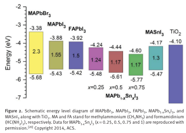
“Bandgap tuning is required to extend the absorption to longer wavelengths without sacrifi cing the absorption coeffi cient. Replacing MA with other organic cations is one approach, since organic cations in the A site of ABX 3 can tune the bandgap because they modify the M–X–M bond length and angle without affecting the valence band maximum.” (Jung and Park, 2015, p. Sec1:12)
“the replacement of MA with formamidinium HC(NH 2 ) 2 + (FA) was found to reduce the bandgap by about 0.07 eV, giving rise to an extension of the absorp- tion wavelength by about 40 nm. [” (Jung and Park, 2015, p. Sec1:12)
“Another approach is the direct modifi cation of M–X bond. For instance, the bandgap decreases from 1.55 eV to 1.17 eV when partially replacing the Pb(2+) in CH 3 NH 3 PbI 3 with Sn(2+)” (Jung and Park, 2015, p. Sec1:12)
“Thus, the bandgap can be tuned in between 1.55 eV and 1.17 eV by varying the ratio of lead to tin.” (Jung and Park, 2015, p. Sec1:12)
“Electron and hole transport properties were reported for CH 3 NH 3 PbI 3 prepared by dif- ferent synthetic methods using a CH 3 NH 3 I + PbI 2 mixture [ 30 ]” (Jung and Park, 2015, p. Sec1:14)
“In the mesoscopic nano- structure, efforts have been made to facilitate charge trans- port by employing new nanomaterials such as ZnO nanorods, 3D-TiO 2 nanoparticles/ITO nanowire composites, and TiO 2 nanoparticle/graphene composites. [ 38–40 ]” (Jung and Park, 2015, p. Sec1:15)
“Recently, an ultrathin MgO nanolayer was found to retard charge recombina- tion between the electrons injected into TiO 2 nanoparticles and the holes in perovskite materials. [ 41 ]” (Jung and Park, 2015, p. Sec1:15)
“Yang's group modifi ed the ITO layer with polyethyleneimine ethoxylate (PEIE) to reduce the work function and increase the carrier density by doping yttrium into the TiO 2 compact layer, thereby improving the electron transport channel in the planar structure perovskite solar cell. [ 42 ]” (Jung and Park, 2015, p. Sec1:15)
“Zhang et al. also inserted polyelectrolyte interme- diate layers such as PEIE and P3TMAHT and achieved a high effi ciency of 12%, which was attributed to the forma- tion of surface dipoles, thereby reducing the work function of the subsequently deposited metal. [ 43 ]” (Jung and Park, 2015, p. Sec1:15)
“HTM-free structure with an FTO/2D sheet TiO 2 /CH 3 NH 3 PbI 3 /Au confi guration showed a PCE of 5.5%, [ 44 ]” (Jung and Park, 2015, p. Sec1:15)
“HTM-free perovskite solar cell was dependent on the depletion layer width at the TiO 2 -CH 3 NH 3 PbI 3 junction” (Jung and Park, 2015, p. Sec1:15)
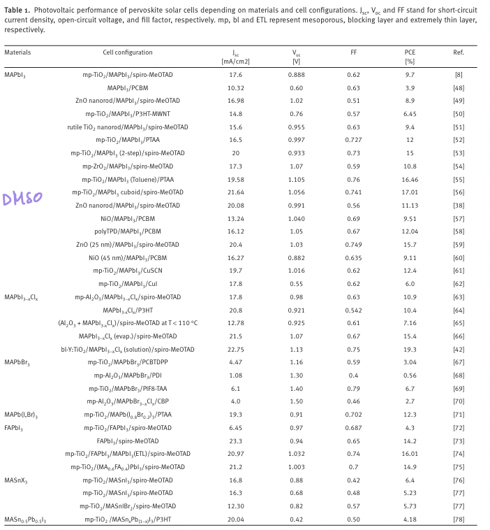
“The studied materials for perovskite solar cells
are CH 3 NH 3 PbI 3 , CH 3 NH 3 PbI 3-x Cl x , CH 3 NH 3 PbBr 3 ,
CH 3 NH 3 Pb(I 1-x Br x ) 3 , HC(NH 2 ) 2 PbI 3 , HC(NH 2 ) 2 Pb(I 1-x Br x ) 3
and CH 3 NH 3 SnI 3 .” (Jung and Park, 2015, p. Sec1:15) Perovskite material studied for solar cell
“HTM materials are also important for high effi ciency per- ovskite solar cells, where the most studied HTM is spiro- MeOTAD, but polymertic HTMs such as the thiophene derivative P3HT and tryarylamine-based PTAA have also been tested.” (Jung and Park, 2015, p. Sec1:15)
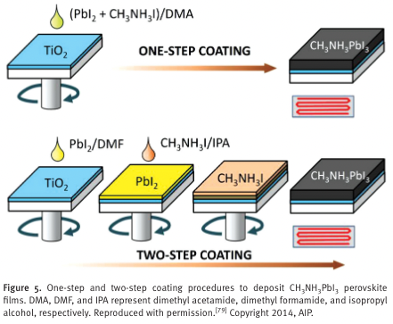
“For the one-step coating method, CH 3 NH 3 I and PbI 2 are dissolved in an appropriate solvent such as a polar aprotic solvent like N,N -dimethylformamide (DMF), gamma- butyrolactone (GBL), or dimethyl sulfoxide (DMSO), and this is used as a coating solution.” (Jung and Park, 2015, p. Sec1:15)
“For the two-step coating method, PbI 2 solution is fi rst coated on the substrate to form a PbI 2 fi lm and then a 2-propanol solution of CH 3 NH 3 I is spun on the PbI 2 fi lm.” (Jung and Park, 2015, p. Sec1:15)
“It was found that the size of CH 3 NH 3 PbI 3 was signifi cantly altered by the concentration of CH 3 NH 3 I in the second deposition step. [ 56 ] W” (Jung and Park, 2015, p. Sec1:15)
“When the concentration of the 2-propanol solution of CH 3 NH 3 I decreased from 0.063 M to 0.038 M, the average CH 3 NH 3 PbI 3 crystal size increased from about 90 nm to about 700 nm, as shown in Figure 6 .” (Jung and Park, 2015, p. Sec1:15)
“Wu et al. successfully dissolved” (Jung and Park, 2015, p. Sec1:15)
“PbCl 2 salt in DMF with an addition of PbI 2 and then coated the mixture onto the mesoporous TiO 2 layer. After exposing it to CH 3 NH 3 I solution, fi nally a CH 3 NH 3 PbI 3-x Cl x per- ovskite layer with controlled morphology was successfully obtained. [ 80 ]” (Jung and Park, 2015, p. Sec1:16)
“It was found that the photovoltaic performance was strongly infl uenced by the CH 3 NH 3 I concentration, i.e., the crystal size of CH 3 NH 3 PbI 3 .” (Jung and Park, 2015, p. Sec1:16)
“Low charge extraction is likely to lead to not only low photocurrent but also a low Fermi level, which can affect V oc .” (Jung and Park, 2015, p. Sec1:17)
“Cheng et al. reported that a single-step process was capable of fabricating fl at and uniform perovskite fi lms by immediately exposing the wet perovskite layer to chlorobenzene, which induced fast crystallization of the perovskite layer. [ 82 ]” (Jung and Park, 2015, p. Sec1:17)
“The role of chlo- robenzene is to rapidly reduce the solubility of perovskite materials in the mixed DMF solvent,” (Jung and Park, 2015, p. Sec1:17)
“Seok's group also exploited a novel perovskite deposition technique using solvent engineering. They used a mixed solvent of γ-butyrolactone and dimethylsulphoxide (DMSO) followed by toluene drop-casting, which led to extremely uniform and dense perovs- kite layers. [ 55 ] The role of DMSO was to retard the rapid reaction between PbI 2 and CH 3 NH 3 I, thereby forming a fl at fi lm containing an intermediate compound of CH 3 NH 3 I-PbI 2 -DMSO. The toluene droplet quickly removed excess DMSO solvent from the wet fi lm, which immedi- ately quenched the constituents. Finally, a homogeneous fl at perovskite layer was obtained after annealing at 100 °C. The effi ciency of these devices was 16.2%,” (Jung and Park, 2015, p. Sec1:17)
“Han et al. used a strong coordinating solvent of DMSO to dissolve PbI 2 and fabricated extremely fl at amorphous PbI 2 layers. Consequently, they were able to fabricate a uniform perovs- kite layer with a small distribution of crystal sizes and a fl at surface morphology, which yielded highly reproducible per- ovskite solar cells with a high effi ciency of 13.5%. Effects of additives such as NH 4 Cl on the perovskite fi lm were also characterized. Ding and Zuo recorded a 80.11% fi ll-factor using NH 4 Cl additive, which was found to enhance the crys- tallinity and morphology of perovskite layer. [ 84 ]” (Jung and Park, 2015, p. Sec1:17)
“When measuring solid thin fi lms like the organometal halide perovskite fi lms, in contrast to solution samples, careful measurements should be carried out because the angular distribution of the emitted light is highly sensitive to the refractive index of the material and to the orientation of the emitting dipoles within the fi lm. [ 86 ]” (Jung and Park, 2015, p. Sec1:18)
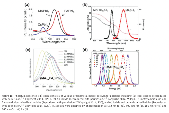
“Lead-based CH 3 NH 3 PbI 3 and HC(NH 2 ) 2 PbI 3 show PL values between 750 and 850 nm, where the maximum PL of HC(NH 2 ) 2 PbI 3 at around 800 nm is red-shifted compared to that of CH 3 NH 3 PbI 3 at around 775 nm (Figure 10 a). [ 19 ]” (Jung and Park, 2015, p. Sec1:18)
“PL quenching measurements are a fast and facile way to
investigate charge separation. In the case where perovskite
is in contact with an electron acceptor (n-type quencher)
or hole acceptor (p-type quencher), PL intensity will be
decreased compared to the isolated state due to charge sepa-
ration by electron or hole injection. From the change in PL
intensity, one can evaluate the degree and effectiveness of
charge separation.” (Jung and Park, 2015, p. Sec1:19) Measure the goodness of the charge separation using PL measurement
“Figure 11 shows the change in PL intensity for the CH 3 NH 3 PbI 3 or CH 3 NH 3 PbI 3-x Cl x perovskites in the absence and presence of n-type or p-type quenchers. A signif- icant decrease in PL intensity is observed when both perovs- kite materials are in contact with electron-accepting PCBM and hole accepting spiro-MeOTAD, as shown in Figures 11 a and b, [ 30,31 ] which is attributed to the injection of electrons and holes.” (Jung and Park, 2015, p. Sec1:19)
“The high-frequency arc is associated with selective contacts, the intermediate-frequency arc is associ- ated with the chemical capacitance, and the low-frequency arc is related to the polarization created by aligning dipoles or dipolar domains to the external electrical fi eld. [ 91 ]” (Jung and Park, 2015, p. Sec1:21)
(Jung and Park, 2015, p. Sec1:22) ITO (Indium tin oxide) vs FTO (fluorin doped tin oxide)
ITO: - 350 C, medium conductivity
FTO: - 600 C, good confuctivity
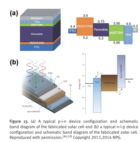
“p-i-n structures (or inverted planar structures)
composed of PEDOT:PSS/perovskite/PCBM architectures” (Jung and Park, 2015, p. Sec1:22) ##Pedot:pss
p-type ZnO
N-type
“n-i-p struc- tures (planar structures) were realized by depositing ZnO ETM at a low temperature (Figure 13 (b)). [ 42,54 ] ZnO nano- materials have also been known to be deposited at below 150 °C.” (Jung and Park, 2015, p. Sec1:22)
“Han et al. reported remarkable progress regarding this stability issue: [ 47 ] they fabricated a HTM-free and triple layer-based perovskite solar cell, composed of a simple mesoscopic TiO 2 /ZrO 2 /C triple layer as a scaffold to host the perovskite absorber. The 10 µm thick carbon back contact layer played an important role in resistance to water.” (Jung and Park, 2015, p. Sec1:23)