Diffusive and Drift Halide Perovskite Memristive Barristors as Nociceptive and Synaptic Emulators for Neuromorphic Computing
(2021) - Rohit Abraham John, Natalia Yantara, Si En Ng, Muhammad Iszaki Bin Patdillah, Mohit Rameshchandra Kulkarni, Nur Fadilah Jamaludin, Joydeep Basu, Ankit, Subodh G. Mhaisalkar, Arindam Basu, Nripan Mathews
- Link:
- DOI: 10.1002/adma.202007851
- Zotero Link: Diffusive and Drift Halide Perovskite Memristive Barristors as Nociceptive and Synaptic Emulators for Neuromorphic Computing
- Tags: #paper
- Cite Key: [@johnDiffusiveDriftHalide2021a]
- Linked notes: Paper Annotations
Abstract
With the current research impetus on neuromorphic computing hardware, realizing efficient drift and diffusive memristors are considered critical milestones for the implementation of readout layers, selectors, and frameworks in deep learning and reservoir computing networks. Current demonstrations are predominantly limited to oxide insulators with a soft breakdown behavior. While organic ionotronic electrochemical materials offer an attractive alternative, their implementations thus far have been limited to features exploiting ionic drift a.k.a. drift memristor technology. Development of diffusive memristors with organic electrochemical materials is still at an early stage, and modulation of their switching dynamics remains unexplored. Here, halide perovskite (HP) memristive barristors (diodes with variable Schottky barriers) portraying tunable diffusive dynamics and ionic drift are proposed and experimentally demonstrated. An ion permissive poly(3,4-ethylenedioxythiophene):polystyrene sulfonate interface that promotes diffusive kinetics and an ion source nickel oxide (NiOx) interface that supports drift kinetics are identified to design diffusive and drift memristors, respectively, with methylammonuim lead bromide (CH3NH3PbBr3) as the switching matrix. In line with the recent interest on developing artificial afferent nerves as information channels bridging sensors and artificial neural networks, these HP memristive barristors are fashioned as nociceptive and synaptic emulators for neuromorphic sensory signal computing.
Notes
Annotations (9/23/2022, 12:21:14 PM)
“diffusive memristors have been very recently employed as artificial nociceptors[12]” (John et al., 2021, p. 2)
“Despite impressive pro- gress with lower dimensional and lead-free perovskites, the specific influence of interfacial injection layers and the intrinsic doping within the perovskite layers have not been rationally studied yet.[25]” (John et al., 2021, p. 2)
“here we propose two key interfaces—an ion permissive poly(3,4- ethylenedioxythiophene):polystyrene sulfonate (PEDOT:PSS) interface that promotes diffusive kinetics and an ion source nickel oxide (NiOx) interface that supports drift kinetics to design diffusive and drift memristors, respectively, with methylammonium lead bromide (CH3NH3PbBr3) as the active switching matrix.” (John et al., 2021, p. 2)
“X-ray diffraction (XRD) patterns indicate that the resulting MAPbBr3 films belong to Pm3m space group with a lattice constant of 5.927 Å, in agree- ment with previous reports.[26] Crystallite size of ≈50 nm is obtained from the Scherrer equation and a preferred growth in the ⟨100⟩ plane is observed (Note S1 and Figure S1, Sup- porting Information). The optical bandgap of the material is ≈2.3 eV, determined from both photoluminescence (PL) and absorbance spectra (Note S1 and Figure S1, Supporting Infor- mation).” (John et al., 2021, p. 2)
“sandwiching MAPbBr3 in between hole (HTL) and electron transporting layers (ETL) connected to indium tin oxide (ITO) and aluminium (Al) elec- trodes, respectively.” (John et al., 2021, p. 2)
“1,3,5-triazine-2,4,6-triyl)tris(benzene- 3,1-diyl)tris(diphenylphosphine oxide) (PO-T2T) serves as the ETL,” (John et al., 2021, p. 2)
“two types of HTL are employed, i.e., PEDOT:PSS and NiOx, to create diffusive and drift memristors, respectively.” (John et al., 2021, p. 2)
“NiOx is hypothesized to act as an interlayer promoting drift kinetics via defect-assisted filament formation across the perov- skite/NiOx interface while the ion permissive PEDOT:PSS/ perovskite interface is chosen to build memristors with diffu- sive kinetics.” (John et al., 2021, p. 2)
“Under mild bias application (up to 3 V), higher currents (I) are observed in the reverse scan direction as compared to forward direction for both PEDOT:PSS and NiOx devices (Figure 1b). These current hystereses could be attributed to the migration of ions inside the perovskite films which have been observed widely.[28–31]” (John et al., 2021, p. 2)
“Under forward bias application, negative” (John et al., 2021, p. 2)
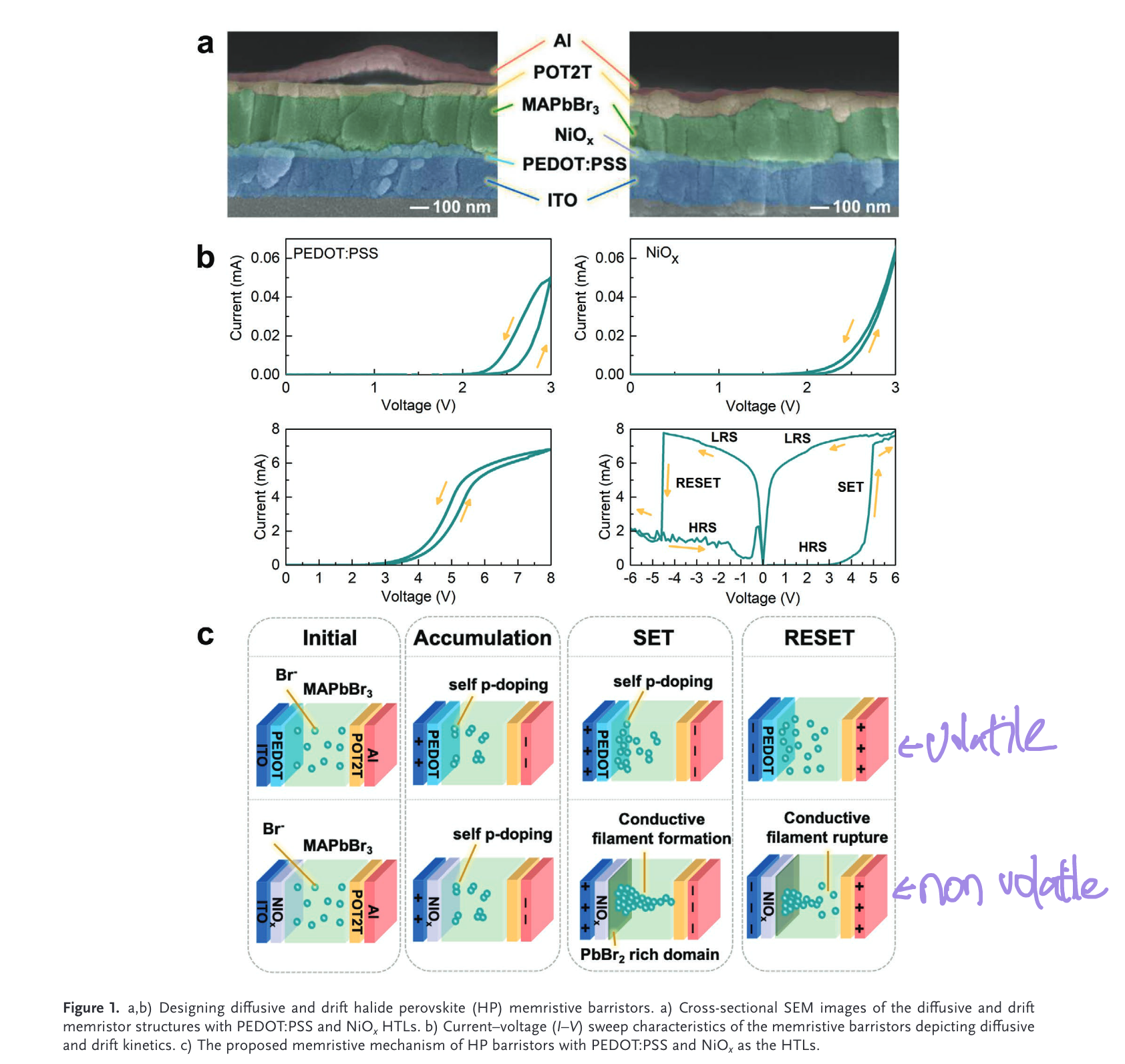
“ions and vacancies (i.e., Br-, VMA-) aggregate and accumulate at the HP-HTL interface to create a self p-type doped region while a self n-doped region is formed at the HP-ETL interface due to the accumulation of positive ions and vacancies (i.e., VBr+, MA+) (accumulation, Figure 1c).” (John et al., 2021, p. 3)
“Larger current hysteresis is observed for PEDOT:PSS devices in this voltage range (0–3 V). This is ascribed to the higher initial hole injection barrier from PEDOT:PSS to the perovskite layer,” (John et al., 2021, p. 3)
“the initial current is recovered upon removing the external bias as ions diffuse back, thus portraying a diffusive volatile threshold behavior for both PEDOT:PSS and NiOx devices under mild bia” (John et al., 2021, p. 3)
“Upon sweeping to higher bias (6 V), the NiOx devices depict a typical bipolar drift nonvolatile memristive behavior switching from a high-resistance state (HRS) to a low-resistance state (LRS) with positive bias application (SET) and vice versa for negative bias application (RESET)” (John et al., 2021, p. 4)
“On the other hand, the PEDOT:PSS devices continue to portray a volatile diffusive memristor behavior even up to 8 V (Figure 1b).” (John et al., 2021, p. 4)
“The nonvolatile behavior of the NiOx devices can be attributed to its ability to support conductive filament formation in the device via ion migration.” (John et al., 2021, p. 4)
“In HPs, these filaments are most likely formed by halogen vacancies.[32]” (John et al., 2021, p. 4)
“Interestingly, the LABE images indicate the growth of white domains (high density materials) starting at the HTL/ perovskite interface for the NiOx devices after bias applica- tion (Figure 2 and Figure S3, Supporting Information). This is attributed to PbBr2-rich perovskite domains as explained below.” (John et al., 2021, p. 4)
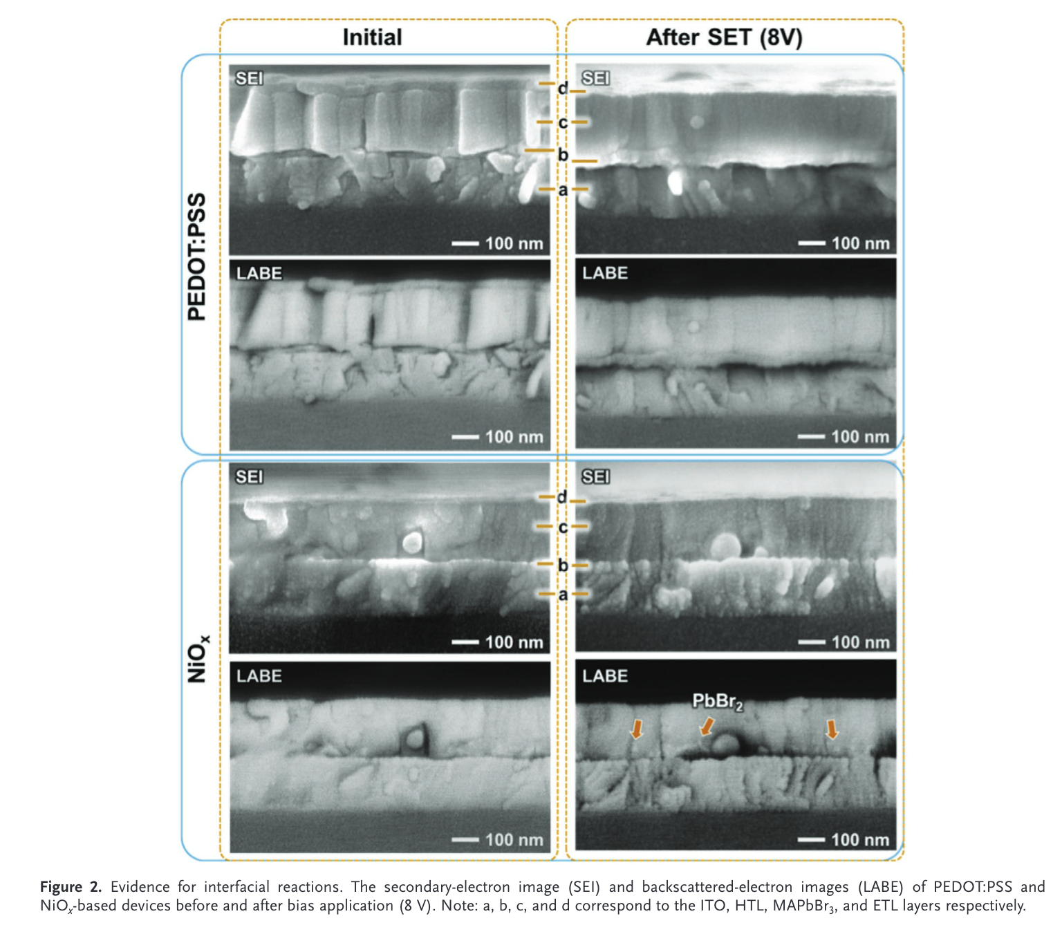
“In conclusion, the NiOx/perovskite inter- face reaction that promotes deprotonation of MABr and oxida- tion of Br- anion could increase the number of ionic defects, increasing the probability of conductive filament formation in the system. In contrast, the more stable PEDOT:PSS/perovskite interfaces have less ionic defects upon external bias application which reduces the probability to form conductive filaments.” (John et al., 2021, p. 5)
“In sum- mary, the ion permissive PEDOT:PSS interface promotes dif- fusive kinetics of ions in the perovskite, while the ion source NiOx interface supports drift kinetics and enables conductive filament formation, resulting in volatile diffusive and nonvola- tile drift memristive barristors, respectively.” (John et al., 2021, p. 5)
“Highly intense noxious stimuli increase their sensitivity semipermanently, finally resulting in “tissue damage” or “sensitization.”[41] In the injured or sen- sitized state, they recalibrate their threshold (decrease) and response (increase) to overprotect the injured site, thereby reducing the latency of emergency response. These phenomena of decreasing the pain threshold and increasing the response are called “allodynia” and “hyperalgesia,” respectively.[42]” (John et al., 2021, p. 5)
“Arrival of nox- ious-like a.k.a. warning stimuli (Vwarn = 4 V, pw ≥ 1.5 s) causes threshold switching of the nociceptor, and the nociceptor out- puts responses above the warning (Iwarn = 8 µA) threshold to warn the system of possible ensuing noxious stimuli. The noci- ceptor enters the “relaxation” phase or alarmed state during which it recalibrates (increases) its sensitivity for a short-while to cater to the often repeated nature of such stimuli, but soon returns to its normal-state if noxious stimuli do not follow immediately. For example, innocuous stimuli (Vsensory ≤ 3 V, pw = 16 ms) closely following (interval ≤ 20 ms) the warning stimuli (Vwarn = 4 V, 1.5 s ≤ pw < 3 s) generate responses above the warning (Iwarn = 8 µA) threshold and sustain the system in the alarmed state, while innocuous stimuli arriving after the relaxation interval (≥ 20 ms) generate insignificant responses below the warning threshold, bringing the system back to its normal state” (John et al., 2021, p. 6)
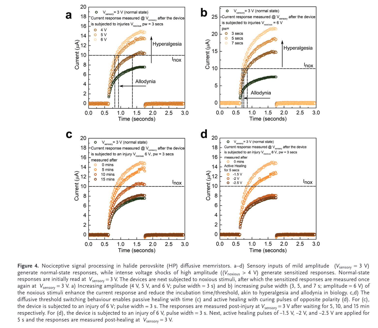
“Detailed electrical characteriza- tions reveal increased baseline currents upon injury, implying a semipermanent change in the device conductance, possibly because of the continuously diminishing hole-injection barrier at the HP-PEDOT:PSS interface due to increased self p-doping.” (John et al., 2021, p. 7)
“From a device mechanism perspective, “hyperalgesia” and “allodynia” could be attributed to the self p- and n-doping effects within the HP layer and doping of the interlayers via ion diffusion in the memristive barristors.” (John et al., 2021, p. 7)
“The passive healing pro- cess points to the back diffusion of ions within the HP layer due to the built-in potential of the barristor, while the active healing process could be attributed to the redistribution of ions in the HP layer and modification of the interfacial barriers with the opposite bias.” (John et al., 2021, p. 7)
“In comparison, CMOS-based implementation of a single nociceptor would require six transistors and one capacitor to implement its adapt- ability to repeated noxious stimuli.[13]” (John et al., 2021, p. 8)
“As supposed to the DC bias scheme which results in a binary digital switching logic (Figure 1b), spike-based write and erase operations without any compliance current control are adopted to iden- tify stable intermediate resistance states and efficiently map the analog and digital switching regimes.” (John et al., 2021, p. 8)
“Input pulses of amplitude +3 to +6 V maps the potentiation window, while -3 to -6 V records the depression window.” (John et al., 2021, p. 8)
“No significant switching is observed for potentiation operations below the threshold of +3.5 V. Higher voltages between +4 and +5.5 V exhibit more gradual and analog increments, subsequently approaching a plateau or soft conductance boundary (Figure 5b).” (John et al., 2021, p. 8)
“Program-
ming voltages higher than +5.5 V result in abrupt conductance
updates and exhibit a digital switching characteristic, indicating
the trade-off between analog weight updates and dynamic
range.” (John et al., 2021, p. 8) Between 5.5 and 6 in figure 5b
“classified into three different operating regimes as “no switching”, i.e., < 3.5 V, +4 V ≤ “gradual analog switching” ≤ +5.5 V, and “digital deterministic switching” > +5.5 V.” (John et al., 2021, p. 8)
“Such digital opera-
tions have little use as synaptic connections utilized to store
analog weights.” (John et al., 2021, p. 8) Maintain the weight is more important than achieving 0-1 digital switching
“Therefore, the trade-off between conductance window and analog programmability requires the optimiza- tion of programming pulse voltages for synaptic operations.” (John et al., 2021, p. 8)
“To account for the analog programming window, we employ a two-parameter multiplicative update model to capture further insights.[44] For normalized synaptic weights denoted between 0 and 1, the following generalized soft bound equations are adopted for incremental and decremental weight changes in potentiation and depression events, respectively δ α w w( ) = - ( ) 1 w γ + (1) δ α w w( ) = wγ -” (John et al., 2021, p. 8)
“where α is a multiplicative parameter which indicates the magnitude of weight modification and γ reflects the nature of boundary approach of the weight update.” (John et al., 2021, p. 8)
“+5 V as the potentiation voltage shows the smallest α and highest γ.” (John et al., 2021, p. 8)
“high α indicates an abrupt initial step with poor distribution across the conductance window, whereas a smaller α ensures more programmable conductance states with 1/α intervals.” (John et al., 2021, p. 8)
“Similarly, a high γ indicates a stronger deviation from linearity, ensuring a more gradual increment toward the conductance boundaries at the expense of dynamic range.” (John et al., 2021, p. 8)
“Although the pro- gramming voltage of +5.5 V produces a larger memory window, +5 V with a smaller α and higher γ portray a wider analog window with gradual incremental weight updates, thus making it the optimal voltage for softly bounded analog operations.” (John et al., 2021, p. 8)
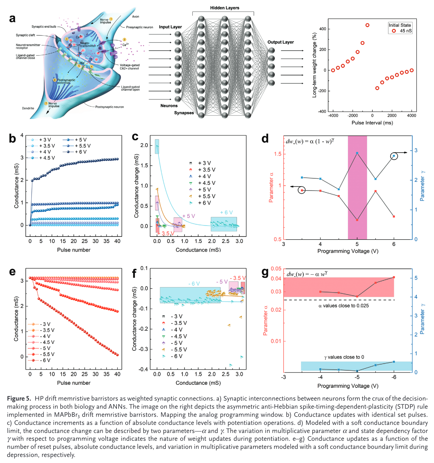
“Depression operations produce highly linear weight updates as shown in Figure 5e. This asymmetry is also reflected in the wider conductance distribution with similar program- ming amplitudes in Figure 5f as compared to the poten- tiation operations in Figure 5c.” (John et al., 2021, p. 9)
“Furthermore, the conductance increments are modeled” (John et al., 2021, p. 9)
“to be highly linear as shown in Figure 5g. As a reference, a perfectly linear conductance update would have an α = 1/40 = 0.025 with evenly distributed conductance updates and γ = 0 with no state dependence nor soft boundary.” (John et al., 2021, p. 9)
“In summary, we expect to extract gradual weight updates from our HP memristive barristor across +4 to +5.5 V for potentiation operations and -4 to -6 V for depression. This indicates the limited window for true analog weight updates, ideal for ANNs.” (John et al., 2021, p. 10)
“spike-timing-dependent-plas- ticity (STDP) rule—a bio-plausible unsupervised learning mechanism that manipulates synaptic weights based on the temporal correlations between pre- and postsynaptic spike timings. In ANNs, the STDP rule is most commonly used in a layer-wise manner to train the convolutional kernels to enable them to self-learn (unsupervised) features from input spike patterns locally.” (John et al., 2021, p. 10)
“Temporal cor- relations between the pre- and postsynaptic spikes create voltage-dependent changes in conductance/weight, estab- lishing an asymmetric anti-Hebbian STDP rule—a causal temporal order of presynaptic activity followed by postsyn- aptic activity leads to long-term depression while the reverse order leads to long-term potentiation (Figure 5a and Note S3 and Figure S14, Supporting Information).” (John et al., 2021, p. 10)
“We report the first diffusive HP memristor and artificial noci- ceptor to the best of our knowledge. The intrinsic migration of ions dopes and dedopes the PEDOT:PSS interface facilely to enforce volatile thresholding functions such as “relaxation,” “sensitization,” and “no adaptation.”” (John et al., 2021, p. 11)
“our results prove the feasibility of utilizing the intrinsic migra- tion and back-diffusion of ions and vacancies unique to HPs, as a proxy to achieve the same.” (John et al., 2021, p. 12)
“5. Experimental Section Devices Fabrication: Indium tin oxide (ITO, 7 Ω cm-2) coated glass substrates were cleaned by sequential sonication in decon soap, distilled water, and isopropanol solution. Substrates were dried and exposed to oxygen plasma for 15 min. Two types of HTL were fabricated, i.e., NiOx and PEDOT:PSS. To deposit NiOx layer, equimolar solution (0.5 m)” (John et al., 2021, p. 12)
“of nickel nitrate hexahydrate and ethylene diamine in ethylene glycol solvent was spun coated (6000 rpm for 60 s), followed by annealing at 300 °C for 1 h in ambient atmosphere. PEDOT:PSS films were deposited by spin-coating (4000 rpm for 60 s) the precursors (Clevios, Al 4083) and followed by annealing at 150 °C for 15 min. Films were then transported into argon filled glovebox for perovskite deposition. Equimolar (1 m) PbBr2 and CH3NH3Br in mixed dimetyl formamide/ dimethyl sulfoxide solvent (3:1) were used as the perovskite precursors. Perovskite films were deposited via spin coating (5000 rpm for 30 s) and an antisolvent (toluene) was introduced 5 s after the spinning start to promote fast nucleations. Approximately 40 nm of POT2T, 1 nm LiF, and 100 nm Al were thermally evaporated in sequence to complete the device fabrication. Shadow masks with active area of 8 mm2 were used during electrode deposition. Devices were then encapsulated inside glovebox and tested in ambient atmosphere.
Characterizations: Bruker D8 advance diffractometer with 0D LynxEYE detector was used to record the XRD pattern of the films. Field effect scanning electron microscope (FE-SEM, JEOL J7600F) were utilized to capture the topographical and cross-sectional images. Absorption and steady-state PL spectra were collected using Shimadzu UV-3600 UV-vis– NIR spectrophotometer and Horiba Fluoromax-4, respectively. Impedance measurements were carried out using Autolab 302N. UPS (Kratos AXIS Supra) with He plasma at excitation energy of 21.22 eV was used to probe the valence band and work function position of the materials.” (John et al., 2021, p. 12)