One-Year stable perovskite solar cells by 2D/3D interface engineering
(2017) - G. Grancini, C. Roldán-Carmona, I. Zimmermann, E. Mosconi, X. Lee, D. Martineau, S. Narbey, F. Oswald, F. De Angelis, M. Graetzel, Mohammad Khaja Nazeeruddin
- Link:
- DOI: 10.1038/ncomms15684
- Zotero Link: One-Year stable perovskite solar cells by 2D/3D interface engineering
- Tags: #paper
- Cite Key: [@granciniOneYearStablePerovskite2017]
- Linked notes: Paper Annotations
Abstract
Despite the impressive photovoltaic performances with power conversion efficiency beyond 22%, perovskite solar cells are poorly stable under operation, failing by far the market requirements. Various technological approaches have been proposed to overcome the instability problem, which, while delivering appreciable incremental improvements, are still far from a market-proof solution. Here we show one-year stable perovskite devices by engineering an ultra-stable 2D/3D (HOOC(CH2)4NH3)2PbI4/CH3NH3PbI3 perovskite junction. The 2D/3D forms an exceptional gradually-organized multi-dimensional interface that yields up to 12.9% efficiency in a carbon-based architecture, and 14.6% in standard mesoporous solar cells. To demonstrate the up-scale potential of our technology, we fabricate 10 × 10 cm2 solar modules by a fully printable industrial-scale process, delivering 11.2% efficiency stable for >10,000 h with zero loss in performances measured under controlled standard conditions. This innovative stable and low-cost architecture will enable the timely commercialization of perovskite solar cells.
Notes
Annotations (1/3/2023, 12:27:00 PM)
“Whenexposed to moisture, the perovskite structure tend to hydrolyse6, undergoing irreversible degradation and decomposing back into the precursors, for example, the highly hygroscopic CH3NH3XandCH(NH2)2X salts and PbX2,withX¼ halide, a process that can be dramatically accelerated by heat, electric field and ultraviolet exposure7,8.” (Grancini et al., 2017, p. 2)
“Material instability can be controlled to a certain extent using cross-linking additives9 or by compositional engineering10,thatis, adding a combination of Pb(CH3CO2)2 3H2OandPbCl2 in the precursors11 or using cation cascade, including Cs and Rb cations, as recently demonstrated2,3, to reduce the material photo-instability and/or optimize the film morphology.” (Grancini et al., 2017, p. 2)
“proper device encapsulation12–14 using buffer layers between perovskite and HTM15 or moisture-blocking HTM16 such as NiOx (ref. 17) delivering, in this case, up to 1,000 h stability at room temperature.” (Grancini et al., 2017, p. 2)
“On the other hand, two-dimensional (2D) perovskites have recently attracted a substantial interest due to their superior stability and water resistance, far above their three-dimensional (3D) counterpart14,20,21. In this respect, solar cells based on the quasi-2D (BA)2(MA)2Pb3I10 (BA ¼ n-butylammonium) perovskite have recently shown 12% efficiency21.” (Grancini et al., 2017, p. 2)
“we have first realized a lowdimensional perovskite using the protonated salt of aminovaleric acid iodide (HOOC(CH2)4NH3I, AVAI hereafter), as the organic precursor mixed with PbI2 (see Supplementary Information for details), following the procedure of the previous work of few of us23,26.” (Grancini et al., 2017, p. 3)
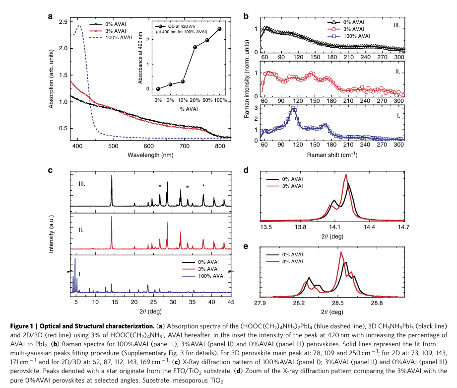
“The deposition results in the formation of a low-dimensional perovskite possibly arranging into a (HOOC(CH2)4NH3)2PbI4 structure.” (Grancini et al., 2017, p. 3)
“The structural properties of the (HOOC(CH2)4NH3)2PbI4 are investigated by Raman spectroscopy and X-ray diffraction.” (Grancini et al., 2017, p. 3)
“he X-ray diffraction measurement of the 100%AVAI perovskite, Fig. 1c (panel I), collected on an extended range down to 3°, exhibits a rich diffraction pattern at low angles with a strong dominant peak at 4.7° along with two lateral peaks at 4.2 and 5.2°. The data provide evidence of the formation of a low-dimensional perovskite with a possible much more complex crystal structure as evident by the multiple reflections at low angles (2yo10o)24,25,30.” (Grancini et al., 2017, p. 3)
“The mixed films obtained by varying the precursors ratio absorb across the whole visible region with an edge at 760 nm and a peak around 430 nm, see Fig. 1a and Supplementary Fig. 4.” (Grancini et al., 2017, p. 3)
“Figure 1a shows the results for the film obtained by 3% AVAI, representing the optimized concentration for the best performing device (see below). The absorption band edge matches with that of 3D CH3NH3PbI3 perovskite, while the peak at 430 nm, which linearly gains intensity upon increasing the AVAI% (see inset in Fig. 1a and Supplementary Fig. 4), resembles the absorption peak of the 2D perovskite, although partially red-shifted.” (Grancini et al., 2017, p. 3)
“The addition of 3% AVAI thus induces the formation of a mixed 2D/3D composite, partly retaining the features of its 2D and 3D constituents.” (Grancini et al., 2017, p. 3)
“Figure 1b compares the Raman spectrum of the 100%AVAI sample with those from the 0%AVAI and the optimized 3% AVAI sample. Additional data at different AVAI concentration are reported in Supplementary Figs 5 and 6. The spectrum of the 2D/3D 3%AVAI composite shows well-defined Raman lines spectrally matching the 2D peaks and standing out of a broader band that is characteristic of the modes of the inorganic lattice of the 3D CH3NH3PbI3 (refs 28,29). In the 3% AVAI sample, sharp Raman features with reduced broadening are identified, suggesting an overall more ordered crystal rearrangement of the 2D/3D film compared with the pure 3D phase.” (Grancini et al., 2017, p. 3)
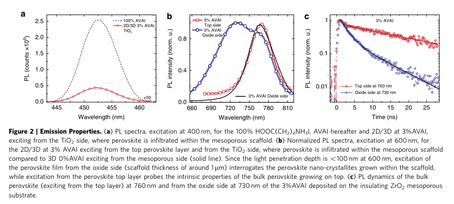
“The PL measured when exciting from the oxide side reveals a weak emission around 450 nm, matching with the one of (HOOC(CH2)4NH3)2PbI4 (Supplementary Figs 2 and 10a). This suggests the presence of a 2D phase mostly retained at the interfacewiththeoxideduetothefavourableanchoringofthe carboxylic acid group of the AVAI ligand to the TiO2 scaffold31.” (Grancini et al., 2017, p. 4)
“Monitoring a more extended spectral window, Fig. 2b, excitation of the bulk top layer results in a single PL peak at 760 nm, as one would expect, while excitation from the oxide side leads to a peak at 730 nm along with a shoulder at 760 nm.” (Grancini et al., 2017, p. 4)
“The emission at 730 nm suggests that a different perovskite phase with a larger band-gap (of 1.69 eV) is formed within the oxide scaffold, but only in the presence of the AVAI precursor.” (Grancini et al., 2017, p. 4)
“Ifwedeposita thicker oxide scaffold, avoiding the formation of the bulk CH3NH3PbI3 perovskite capping layer, only the peak at 730 nm appears (Supplementary Figs 9, 10), confirming that the emission at 760 nm comes from the bulk perovskite.” (Grancini et al., 2017, p. 4)
“Indeed, if the 3% AVAI perovskite is deposited on a compact glass substrate the blue-shifted emission peak at 730 nm is not observed, while only the emission at around 760 nm is visible, independently from the excitation side (see Supplementary Figs 12,13 and the discussion in Supplementary Information).” (Grancini et al., 2017, p. 4)
“These results suggest that the 2D/3D interaction widens the 3D perovskite band-gap in the interface region. Additionally, the thin 2D layer does not constitute a barrier to electron injection to TiO2, but it rather constitutes a barrier towards electron recombination, since the 2D conduction band is found at lower energy than that of the 3D CB. This result is confirmed also in the presence of spin-orbit-coupling, see PDOS in Fig. 3c and Supplementary Fig. 14.” (Grancini et al., 2017, p. 4)
“The results indicate that the 2D/3D perovskite organizes in a gradual multi-dimensional structure” (Grancini et al., 2017, p. 4)
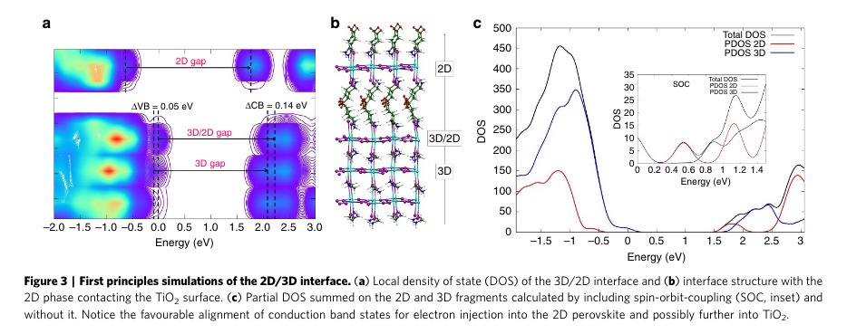
“retaining the individual 2D and 3D phases, but, importantly also templating the formation of a novel oriented CH3NH3PbI3 phase stabilized at the 2D/3D interface.” (Grancini et al., 2017, p. 5)
“based on the pioneering work by Mei et al.23” (Grancini et al., 2017, p. 5)
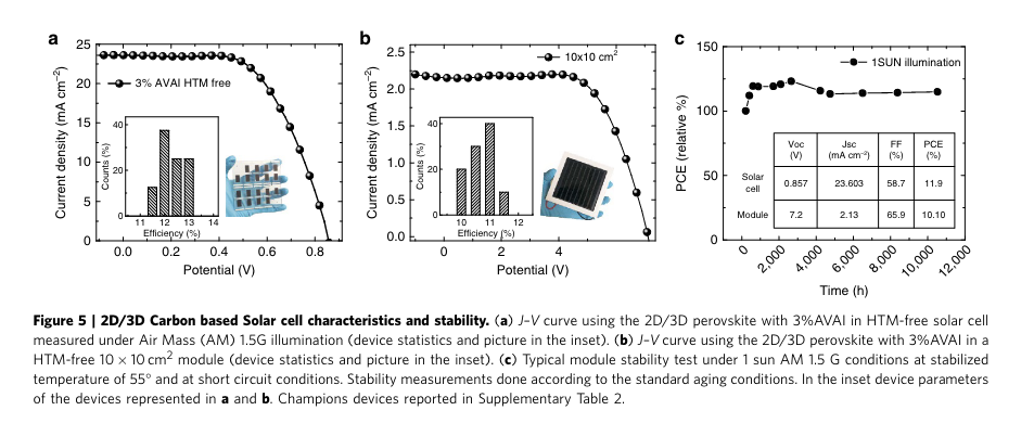
“We have tested the modules under different conditions under simulated AM 1.5 G solar illumination at 1000 W m 2 and cycling of temperature up to 90 C under ambient conditions, in agreements with the standards (Supplementary Fig. 17). The results, in Fig. 5c, show an extraordinary long-term stability of 410,000 h and excellent response at elevated temperature (Supplementary Fig. 17), reported here for the first time. I” (Grancini et al., 2017, p. 5)
“It is fair to notice that an initial increase is detected in Fig. 5c in the first 500 h of the stability test. This can be due to concomitant effects such as light or field induced ion movement with the associated structural rearrangement, light-induced trap formation, or interfacial charge accumulation that can alter the device behaviour (and also cause the device hysteresis), at present under intense scrutiny37,43,44.” (Grancini et al., 2017, p. 5) Initial increase in performance due to.... What cause of initial performance increase
“In conclusion, we interface engineering a built-in 2D/3D perovskite which grows forming a peculiar bottom-up phase- segregated graded structure.” (Grancini et al., 2017, p. 6)
“The unique combination of the 2D layer acting as a protective window against moisture, preserving the 3D perovskite and of the efficient 3D one provides the hint for the development of a stable perovskite technology, paving the way for the realization of near term high efficient and stable perovskite solar cells for widespread deployment.” (Grancini et al., 2017, p. 6)
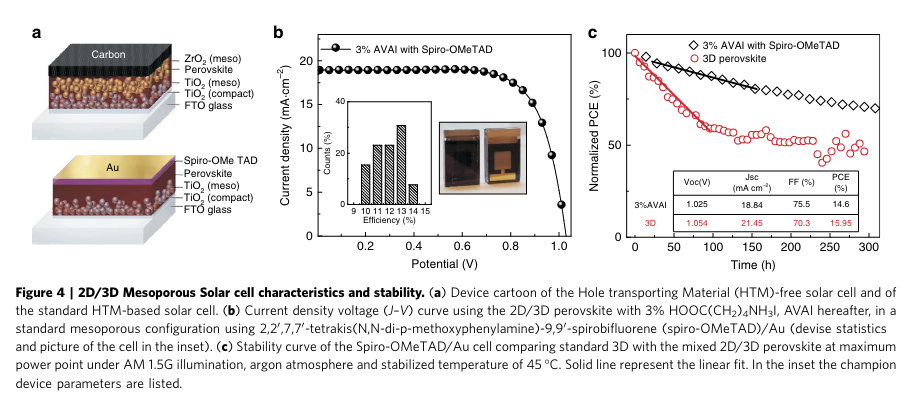
“Fabrication of carbon-based mesoscopic solar cells. The FTO glass was first etched to form two separated electrodes before being cleaned ultrasonically with ethanol. Then, the patterned substrates were coated by a compact TiO2 layer by aerosol spray pyrolysis, and a 1 mm nanoporous TiO2 layer was deposited by screen-printing of a TiO2 slurry, which was prepared as reported previously23.
After being sintered at 450 C for 30 min, a 2 mm ZrO2 spacer layer was printed on the top of the nanoporous TiO2 layer using a ZrO2 slurry, which acts as an insulating layer to prevent electrons from reaching the back contact. Finally, a carbon black/graphite counter electrode with a thickness of about 10 mm was coated on top of the ZrO2 layer by printing a carbon black/graphite composite slurry, and sintering at 400 C for 30 min. After cooling down to room temperature,” (Grancini et al., 2017, p. 6)
“the perovskite precursor solution was infiltrated through a semi-continuous printing process from the top of the carbon counter electrode by drop casting. The complete printing process was carried out in air conditions. After drying at 50 C for 1 h, the mesoscopic solar cells containing perovskite was obtained. The perovskite precursor solution was prepared as follows: for the 3D precursor solution, 1.2 M of MAI and 1.2 M of PbI2 were dissolved in g-butyrolactone, and then stirred at 60 C overnight. For the 2D perovskite 1.2 M of AVAI and 1.2 M of PbI2 were dissolved in g-butyrolactone and then stirred at 60 C overnight.
The (AVA)x(MA)1-xPbI3 precursor solution was prepared in the same manner except that a mixture of (AVAI:PbI2) and (MAI:PbI2) with 3, 10, 20, 50 vol% (that is, (AVAI:PbI2)/((AVAI:PbI2) + (MAI:PbI2))) was used. All the cells were encapsulated in ambient atmosphere to protect the cell from mechanical damage, with no special control on the humidity and oxygen content. The encapsulation was performed by covering the cells with a thin glass and sealing the edges using DuPont Surlyn polymer. In the case of the modules, the same process was carried out but adding an extra ring of epoxy glue around the cell as a second protection.” (Grancini et al., 2017, p. 6)
mixing "...except that a mixture of (AVAI:PbI2) and (MAI:PbI2) with 3, 10, 20, 50 vol%"
2 solution
(AVAI:PbI2) = (1.2 M AVAI + 1.2 M PbI2) di GBL
(MAI:PbI2) = (1.2 M MAI + 1.2 M PbI2) di GBL
trus di mixing keduanya
zotero-ed (2023/1/3)