Carbon-based materials for stable, cheaper and large-scale processable perovskite solar cells
(2019) - Lucia Fagiolari, Federico Bella
- Link:
- DOI: 10.1039/C9EE02115A
- Zotero Link: Carbon-based materials for stable, cheaper and large-scale processable perovskite solar cells
- Tags: #paper
- Cite Key: [@fagiolariCarbonbasedMaterialsStable2019]
- Linked notes: Paper Annotations
Abstract
Replacing gold and boosting stability: carbon as Holy Grail for perovskite solar cells. , Almost ten years after their first use in the photovoltaic (PV) field, perovskite solar cells (PSCs) are now hybrid devices that, in addition to having reached silicon performance, can accelerate the energy transition and boost the use of abundant elements for their manufacturing process. However, noble metals (in particular gold) represent the most typically used sources for back electrode fabrication, and this issue has been intensively considered by the research community in the last five years. This review shows how the most promising solution, considering also the need to develop a large-scale production process, is based on the use of carbon-based materials for the preparation of back electrodes. Graphite, carbon black, graphene and carbon nanotubes (CNTs) have been proposed, functionalized and characterized, leading to laboratory-scale solar cells and modules capable of providing excellent efficiencies and ensuring stability greater than those of gold-based devices. Strengthened by these results and its hydrophobizing properties, carbon has also started to be used as an electron transporting material (ETM), with excellent results on both rigid and flexible substrates. This review discusses the major advances and the updated state-of-the-art in the carbon-based PSC scenario, keeping a solid trajectory where the accessibility, low cost, high electrical conductivity, chemical stability and controllable porosity of carbon are highlighted and exploited in the design of upscalable hybrid solar cells.
Notes
Annotations (1/3/2023, 10:27:27 AM)
“For efficient charge extraction, the valence band (VB) and the conduction band of the perovskite should lie below the highest occupied molecular orbital (HOMO) of the HTM and under the lowest unoccupied molecular orbital (LUMO) of the ETM, respectively.58,59” (Fagiolari and Bella, 2019, p. 6)
“Electrons are collected by the ETM and migrate towards the anode side, while holes are collected by the HTM and migrate towards the back electrode” (Fagiolari and Bella, 2019, p. 6)
“HTMs are expensive and require an inert atmosphere for the deposition process.62–64 They are also subjected to halide and metal ion migration,65 resulting in the degradation of the cell.66–68 2,2,7,7-tetrakis(N,N-di-p-methoxy- phenylamine)-9,90-spirobifluorene (spiro-OMeTAD) is commonly used as a HTM in gold-based PSCs.69 It needs to be doped with lithium bis(trifluoromethanesulfonyl)imide (LiTFSI), a hygroscopic and deliquescent salt that allows the penetration of water molecules, leading to the decomposition of the perovskite.70,71” (Fagiolari and Bella, 2019, p. 6)
“perovskite materials show a large carrier path and PSCs can also work without the HTM.72,73” (Fagiolari and Bella, 2019, p. 6)
“In this architecture, an insulating layer, such as Al2O3 or ZrO2, is necessary to keep the front electrode separated from the back one.74” (Fagiolari and Bella, 2019, p. 6)
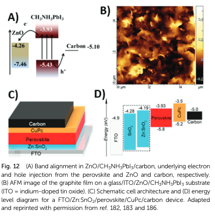
“carbon has a suitable work function of 5.0 eV, very close to that of gold (5.1 eV).29 I” (Fagiolari and Bella, 2019, p. 6)
“all articles on PSCs published before 2012 were focused on devices using liquid electrolytes.” (Fagiolari and Bella, 2019, p. 6)
“Carbon-based devices appeared approximately only one year after the first solid-state PSC based on spiro-OMeTAD.” (Fagiolari and Bella, 2019, p. 6)
“unexpected efficiency improvement that spiro-OMeTAD promoted is sometimes considered the true starting point of the PSC topic.” (Fagiolari and Bella, 2019, p. 6)
“CB is an amorphous nanopowder obtained by incomplete combustion of carbonaceous materials.” (Fagiolari and Bella, 2019, p. 6)
“Even though it shows lower conductivity than graphite, carbon black is used to distort and break the preferential orientation of graphite flakes.” (Fagiolari and Bella, 2019, p. 6)
“the ratio between carbon black and graphite is relevant not only in terms of electrical conductivity; conversely, it also has an influence on the processability of the carbon paste, in terms of viscosity, adhesion to the other cell layers and infiltration degree of the perovskite.76,77” (Fagiolari and Bella, 2019, p. 6)
“Carbon-based materials may be processed by two main deposition techniques. The first process requires temperatures in the range 400–500 1C.58 A mesoporous carbon layer is deposited by doctor-blade or screen-printing techniques on the top of an insulating layer, and subsequently sintered” (Fagiolari and Bella, 2019, p. 6)
“three oxides have been successfully used as insulating layers in the PSC field: ZrO2, 78,79 Al2O3 79,80 and TiO2.
81 The latter can be used both as a compact layer and as a mesoscopic layer, in combination with ZrO2 and Al2O3.
81 Generally speaking, ZrO2 is more efficient as the insulating layer with respect to Al2O3.” (Fagiolari and Bella, 2019, p. 6)
“The effect of the thickness of the insulating layer has been investigated by Liu et al.78 and Barichello et al.80 Optimal thicknesses of 1 mm and 1.8 mm for ZrO2 and Al2O3, respectively, were found.” (Fagiolari and Bella, 2019, p. 6)
“Below these values, most of the generated photoelectrons recombined with holes, leading to a high energy loss. On the other hand, the thickness of the insulating layer should not be higher than the limit of carrier diffusion length.” (Fagiolari and Bella, 2019, p. 6)
“More details on this topic can be found in a recently published review article.82” (Fagiolari and Bella, 2019, p. 6)
“The perovskite phase is formed later, since it is not stable over 120 1C,83 by drop-casting a precursor solution on top of the carbon layer. The perovskite precursor solution must penetrate the entire thickness of the carbon layer, to ensure a contact with the anode. Mesoscopic cells, where a good interface between carbon and the perovskite is established, are obtained by this strategy.” (Fagiolari and Bella, 2019, p. 6)
“However, the penetration is somehow difficult, may require the use of additives and is not applicable to flexible” (Fagiolari and Bella, 2019, p. 6)
“substrates.” (Fagiolari and Bella, 2019, p. 7)
“The other strategy is a layer-by-layer deposition,58 where a perovskite phase is formed by a one- or two-step method and carbon is doctor-bladed or screen-printed on top of CH3NH3PbI3 or HTM.” (Fagiolari and Bella, 2019, p. 7)
“The carbon layer may also be deposited on another substrate and then transferred onto the cell. These depositions are simpler, do not require high temperature and may be suitable also for flexible devices, but the interface usually suffers from poor contact.84–86 Planar architectures with and without HTMs are obtained.” (Fagiolari and Bella, 2019, p. 7)
“spheroidal graphite with better conductivity and favorable morphology for pore filling was used in the carbon composite electrode.” (Fagiolari and Bella, 2019, p. 7)
“As evidenced by cross-sectional scanning electron microscopy (SEM) images, shown in Fig. 2, a more effective pore filling was ensured by the smooth structure of spheroidal graphite.” (Fagiolari and Bella, 2019, p. 7)
“if the carbon layer is too thick, the penetration of the perovskite precursor solution is hindered. As a consequence, a poor contact between carbon and the perovskite phase is established. However, too thin carbon layers do not provide sufficient conductivity. The carbon layer thickness ranged from 5 to 15 mm and it was found that the optimal thickness was 9 mm, with a short-circuit current density ( Jsc) of 18.06 mA cm2 and a remarkable PCE of 11.63%.” (Fagiolari and Bella, 2019, p. 7)
“On the other hand, graphite flakes with different sizes were added to the carbon paste, to further enhance the conductivity of the carbon back electrode.
Dimensions of graphite flakes ranged from 0.5 to 8 mm; it was found that the 8 mm-large sample ensured the best perovskite infiltration, having the biggest pore size. In addition, it had the lower square resistance.” (Fagiolari and Bella, 2019, p. 7)
“Different results were obtained by Raminafshar et al. in 2018.88 They investigated the effect of TiO2, ZrO2 and carbon thickness in HTM-free, high-temperature processed PSCs. Con- cerning the back electrode, the carbon layer should be thin enough to ensure perovskite infiltration; however, too thin layers are mechanically fragile and can crack, with a drop in the conductivity. Four thickness values were tested: 6.5, 15, 25 and 54 mm. On the other hand, the thicknesses of TiO2 and ZrO2 were kept constant at 0.4 and 1.7 mm, respectively. As reported in Table 1, the PCE improved with carbon thickness.
Only when the layer became too thick (54 mm) the PCE dropped due to the poor penetration of the perovskite phase. The best carbon thickness was 25 mm, with an open-circuit voltage (Voc) of 0.88 V, a Jsc of 21.4 mA cm2, a fill factor (FF) of 0.57 and a PCE of 10.7%.” (Fagiolari and Bella, 2019, p. 7)
“It is matter of debate in the scientific community if the carbon layer behaves simply like an electrode ohmic contact or has HTM properties. Indeed, carbon shows a higher work function than other commonly used metals, such as silver and aluminium, and its Fermi level (5.0 eV) is close to the VB maximum of CH3NH3PbI3 (5.4 eV). This makes the hole extraction at the perovskite/carbon interface possible and paves the way to HTM-free PSCs.” (Fagiolari and Bella, 2019, p. 7)
“Du et al., and the main outcome was that the cell voltage was more affected by the perovskite crystallinity than by other factors.89” (Fagiolari and Bella, 2019, p. 7)
“The evaporation of organic solvents was facilitated by the use of high temperature. In this way, a highly mesoporous structure, with pore filling ability, was created. On the other hand, highly resistive electrodes, with poor perovskite infiltration, were formed at temperatures lower than 300 1C. The samples treated at 350 and 400 1C achieved a remarkable PCE of 8.4% and 12.4%, respectively. SEM images showed an increased unifor- mity and a defect-free morphology in high-temperature treated carbon films. Raman spectra underlined the high graphitization degree and the lack of defect regions.” (Fagiolari and Bella, 2019, p. 8)
“Tian et al. in 2018.92 They suggested that a fine regulation of the oxygen content in the carbon black, used to fabricate the back electrode, may be exploited for tuning the work function of carbon and increasing the surface area and the contact with the perovskite phase. Oxygen can be considered as a dopant, since it increases the work function of the material; it can be present as C–OH, COOH and CQO groups on the surface, enlarging the interlayer distance through electrostatic repulsion, thus increasing the surface area.” (Fagiolari and Bella, 2019, p. 8)
“by Hashmi et al. in 2017.96 They reported a humidity-assisted thermal exposure (HTE) as a post-treatment method for PSCs. After the pore filling of the substrate with the perovskite precursor solution (one-step deposition method), the cell was exposed to 70% relative humidity (RH) for 115 h.
This treatment resulted in a drastic enhancement of the preliminarily measured PV parameters. Also, the hysteresis effect was reduced. This beneficial effect may be ascribed to” (Fagiolari and Bella, 2019, p. 9)
“two main factors: first of all, the sheet resistance of the carbon layer, measured by the four-probe sheet resistance method, was found to drastically reduce after the HTE treatment. Water molecules probably increased the interconnectivity between carbon nanoparticles (NPs) and perovskite crystals.” (Fagiolari and Bella, 2019, p. 10)
“Secondly, the hydrophobic carbon impeded the fast intrusion of water drops, that would have led to the decomposition of the perovskite, and allowed only the penetration of gaseous water molecules.” (Fagiolari and Bella, 2019, p. 10)
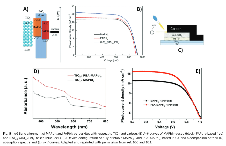
“A suitable strategy to further enhance PSC efficiency is the replacement of a methylammonium (MA) cation98 with 5-amino valeric acid (5-AVA)99 or formamidinium (HC(NH2)2 +, FA).100,101 When 5-AVA is added in the precursor solution, it replaces the MA cation in the cuboctahedral site of MAPbI3. 5-AVA templates the crystallization of the perovskite in the pores of mesoporous TiO2, providing a lower defect concentration,99 while its –COOH and –NH2 groups interact with TiO2 through hydrogen bonding, ensuring a better interfacial contact with the anode” (Fagiolari and Bella, 2019, p. 10)
“FA cation forms a perovskite phase with a band-gap of 1.47 eV, lower than that of MAPbI3 (1.55 eV).” (Fagiolari and Bella, 2019, p. 10)
“Similar to 5-AVA, the phenethylammonium (PEA) cation improved the contact with TiO2 at the interphase, ensured a better pore filling of the solution and lowered the defect concentration in the perovskite film.” (Fagiolari and Bella, 2019, p. 10)
“As demonstrated by time- resolved photoluminescence (PL) spectra,104,105 the exciton life- time in PEA-MAPbI3 was much longer (40 ns) with respect to that in MAPbI3 (12 ns). PEA-MAPbI3 also exhibited a stronger absorption than MAPbI3 in the range 350–800 nm,” (Fagiolari and Bella, 2019, p. 10)
“Despite a remark- able initial PCE of 10%,121 inorganic CsPbI3 underwent an irre- versible transformation toward a non-perovskite phase. Therefore, the stability was seriously compromised.121,122” (Fagiolari and Bella, 2019, p. 10)
“However, the thermal stability can be increased by fully replacing iodide with bromide.123,124 In fact, CsPbBr3 is stable till 580 1C125 and presents great charge transport ability and mean free path.12” (Fagiolari and Bella, 2019, p. 10)
“TiO2 is the most used anodic material not only for PSCs, but also for dye-sensitized solar cells (DSSCs).129–141 It presents several advantages, such as low cost, low toxicity, adequate band-gap and high electron collection efficiency.” (Fagiolari and Bella, 2019, p. 10)
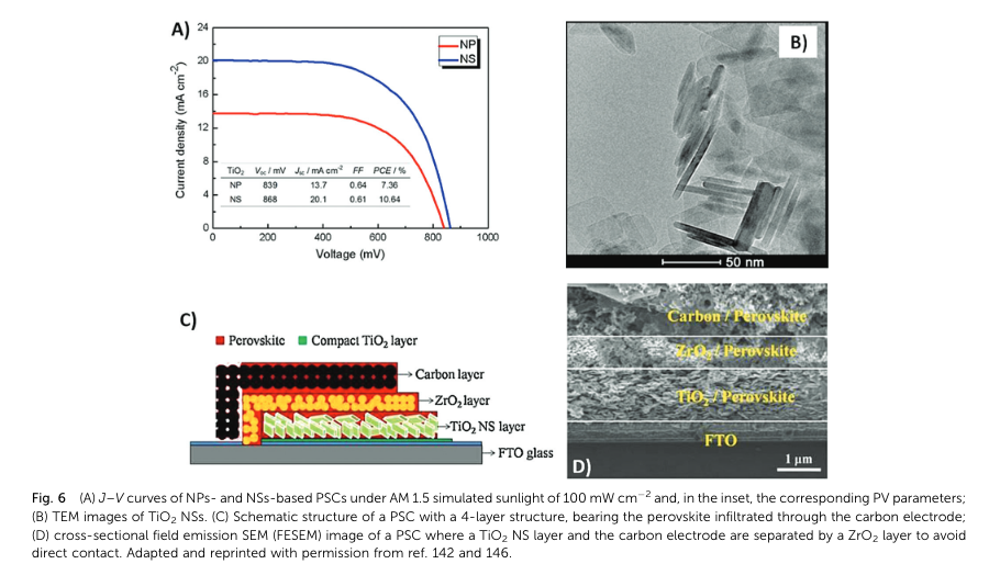
“Zhang et al. in 2018.146 They built two types of 1 mm-thick anodes, one based on TiO2 NSs (see Fig. 6D) and the other one based on TiO2 NPs. The PCE of the NS-based device shown in Fig. 6C was almost twice that of the NP-based one (8.11% vs. 4.37%, respectively), confirming that the (001) anatase facet was more reactive and suitable for perovskite adhesion and electron injection.” (Fagiolari and Bella, 2019, p. 11)
“TiO2. In fact, recombination decreased by increasing the layer thickness, as confirmed by electrochemical impedance spectroscopy (EIS)” (Fagiolari and Bella, 2019, p. 11)
“a too thick TiO2 layer caused high series resistance.” (Fagiolari and Bella, 2019, p. 11)
“In 2015, Liu et al. reported a HTM-free PSC with an organic silane self-assembled between TiO2 and the perovskite.148 The silanization of the anode was achieved by dipping a high-temperature processed TiO2/ZrO2/ carbon substrate and subsequent hydrolysis.” (Fagiolari and Bella, 2019, p. 11)
“In order to replace expensive HTMs, many p-type inorganic semiconductors have been reported. Among them, NiO showed several advantages, such as low cost, stability, wide band-gap and high hole mobility.” (Fagiolari and Bella, 2019, p. 11)
“It was suggested that NiO limited charge recombination and ameliorated hole collection efficiency toward the carbon electrode” (Fagiolari and Bella, 2019, p. 12)
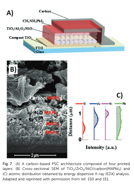
“Xu et al.151 ZrO2 was used as both spacer and insulator to keep the TiO2 anode and NiO semiconductor separated. The resulting TiO2/ZrO2/NiO/carbon(MAPbI3) architecture presented a p–i–n configuration as shown in Fig. 7B and C. Besides enhancing charge collection at the interface with the carbon back electrode, NiO successfully acted also as an electron blocking layer, thus reducing charge recombination.” (Fagiolari and Bella, 2019, p. 12)
“Charge transport in NiO can be attributed to positively- charged nickel vacancies.” (Fagiolari and Bella, 2019, p. 12)
“By increasing the temperature, the removal of some nickel(II) cations results in increasing the number of oxygen atoms surrounding the remaining nickel atoms. For this reason, some nickel(II) are oxidized to nickel(III) and conductivity is attributed to hole hopping from the Ni3+ sites to Ni2+ ones.” (Fagiolari and Bella, 2019, p. 12)
“Carbon atoms in the graphitic layers can be easily replaced by electron-deficient boron by high-temperature thermal treatment with B4C, as shown in Fig. 8A.156,157 After this treatment, the work function of the carbon electrode was improved by the incorporation of the electron-deficient boron atom (5.10 vs. 4.81 eV of pure graphite, PG).” (Fagiolari and Bella, 2019, p. 13)
“Other alternatives to NiO are p-type spinel oxides that are promising HTMs due to their excellent hole mobility. The first use of p-type Co3O4 as the HTM in carbon-based PSCs was reported in 2018 by Bashir et al.158” (Fagiolari and Bella, 2019, p. 13)
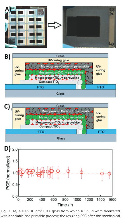
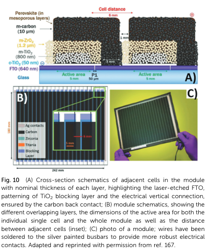
“Further issues for the realization of scalable high-temperature processed carbon-based PSCs are (i) mechanical infiltration of the perovskite solution, in order to have a fully reproducible and printable fabrication method;163 (ii) long-term stability under UV-light soaking;164,165 (iii) high-temperature thermal stability;166 and (iv) enlargement of the active area of the cell.167 T” (Fagiolari and Bella, 2019, p. 14)
“5-AVA iodide was added in the precursor ink to slow down perovskite crystal growth, thus preventing the inkjet printer cartridge from clogging and ensuring a better filling through the carbon layer.” (Fagiolari and Bella, 2019, p. 14)
“PCE of the devices stored under dark conditions was found to initially increase by 13% in the first three weeks. This was ascribed to a further curing of the perovskite phase. Then, the PCE restored to its initial value and remained stable for 1046 h” (Fagiolari and Bella, 2019, p. 14)
“The sluggish degradation of the perovskite, with formation of PbI2, was observed and monitored by the camera imaging technique.” (Fagiolari and Bella, 2019, p. 14)
“stored without encapsulation were subjected to intense 1.5 sun UV light illumination in an electronic weather chamber, at 45% RH and 40 1C.164 In the first 250 h, the cell ameliorated its performances in both Jsc (+17%) and PCE (8.6%); this behavior may be ascribed to the additional curing of perovskite crystals under UV light.” (Fagiolari and Bella, 2019, p. 14)
“Part of the dark-brown perovskite layer became yellow after 751 h, due to the formation of PbI2 and the disappearance of HI and CH3NH2.” (Fagiolari and Bella, 2019, p. 15)
“XRD demonstrated that PbI2 reflections appeared only in epoxy-free aged samples.” (Fagiolari and Bella, 2019, p. 15)
“perovskite undergoes a phase transition from tetragonal to cubic at 54 1C.172” (Fagiolari and Bella, 2019, p. 15)
“suggesting that sealing is a necessary protection against moisture, but it could also cause internal decomposition in the over-sealed configuration.” (Fagiolari and Bella, 2019, p. 15)
“However, during the synthesis of TiO2 by the sol–gel process, the widely used precursor Ti(OC4H9)4 undergoes hydro- lysis under atmospheric conditions, resulting in a non-uniform morphology of TiO2. For these reasons, different amounts of diethanolamine (DEA), whose basic character hampers the” (Fagiolari and Bella, 2019, p. 17)
“hydrolysis of Ti(OC4H9)4, were added in the precursor solution.
SEM images confirmed that the DEA-free TiO2 blocking layer presented many cracks and voids, with a width of E400 nm, that can act as recombination centers. On the other hand, DEA- containing films were compact and homogeneous and fully covered the FTO substrate.” (Fagiolari and Bella, 2019, p. 17)
“Since the carbon back electrode is usually deposited from carbon pastes, the solvent content in the suspension should not be harmful for the underlying layer. For this reason, the effect of the nature of the solvent was investigated. In particular, the lowest and the highest PCEs were found with chlorobenzene and toluene,” (Fagiolari and Bella, 2019, p. 18)
“In addition [6,6]-phenyl-C61-butyric acid methyl ester (PC61BM) and PEDOT:PSS were used as the ETM and HTM, respectively” (Fagiolari and Bella, 2019, p. 23)
“Last, a p-type NiO semiconductor was demonstrated to work as a HTM in carbon-based PSCs.” (Fagiolari and Bella, 2019, p. 23)
“Bashir et al. investigated the stability of a HTM-free device fabricated with a thin layer of copper-doped nickel oxide (Cu:NiOx) NPs, which helped in improving the photocurrent and reducing the recombination resistance.32” (Fagiolari and Bella, 2019, p. 24)
“Almost all of the carbon-based PSCs reported so far have been fabricated using TiO2 as the ETM, the latter requiring a high-temperature sintering process. As an alternative, Zhou et al. proposed solution-processed hexamethonium bromide (HMB)-doped C60 as the ETM, achieving a high PCE of over 16% without hysteresis.326 T” (Fagiolari and Bella, 2019, p. 24)
“Coupling carbon-based electrodes with all-air processing would truly lead to an easily upscalable PSC fabrication procedure.
This goal was achieved by Zhou et al., who prepared MWCNT- incorporated FAxMA1xPbIyBr3y perovskite films in ambient air, where hydrophobic MWCNTs mediated the crystallization of the perovskite and prevented the erosion by moisture.327 With the low annealing temperature (o150 1C) adopted, a PCE of 16.25% was achieved and the photostability of the devices without encapsulation was studied by MPP tracking under continuous 1 sun illumination at a RH of 30–80%.” (Fagiolari and Bella, 2019, p. 24)
“Since the commonly used MAPbI3 photoabsorber is ambient- unstable and incompatible with the low-cost mass-production of carbon-based PSCs, Zhou et al. fabricated (EA)2(MA)n1PbnI3n+1 films (n = 20, 10, 6) and assembled ITO/C60/(EA)2(MA)n1PbnI3n+1/C devices with PCE exceeding 11.88%.60 The photostability was assessed without encapsulation, by MPP tracking under continuous 1 sun illumination (without a cut-off UV filter) in air with a RH of 30–80%. The PCE was retained at 91.8% after 308 h” (Fagiolari and Bella, 2019, p. 25)
“Excess PbI2 is commonly considered as a way to boost the PCE in standard PSCs, and Kapoor et al. checked this issue in fully printable carbon-based devices.329 An improvement in Voc was detected, while other parameters remained unchanged” (Fagiolari and Bella, 2019, p. 25)
Given by Prof. Nripan on 12/8/2022