The application of halide perovskites in memristors
(2020) - Gang Cao, Chuantong Cheng, Hengjie Zhang, Huan Zhang, Run Chen, Beiju Huang, Xiaobing Yan, Weihua Pei, Hongda Chen
- Link:
- DOI: 10.1088/1674-4926/41/5/051205
- Zotero Link: The application of halide perovskites in memristors
- Tags: #paper
- Cite Key: [@caoApplicationHalidePerovskites2020]
- Linked notes: Paper Annotations
Abstract
New neuromorphic architectures and memory technologies with low power consumption, scalability and high-speed are in the spotlight due to the von Neumann bottleneck and limitations of Moore's law. The memristor, a two-terminal synaptic device, shows powerful capabilities in neuromorphic computing and information storage applications. Active materials with high defect migration speed and low defect migration barrier are highly promising for high-performance memristors. Halide perovskite (HP) materials with point defects (such as gaps, vacancies, and inversions) have strong application potential in memristors. In this article, we review recent advances on HP memristors with exceptional performances. First, the working mechanisms of memristors are described. Then, the structures and properties of HPs are explained. Both electrical and photonic HP-based memristors are overviewed and discussed. Different fabrication methods of HP memristor devices and arrays are described and compared. Finally, the challenges in integrating HP memristors with complementary metal oxide semiconductors (CMOS) are briefly discussed. This review can assist in developing HP memristors for the next-generation information technology.
Notes
Annotations (9/5/2022, 9:52:25 AM)
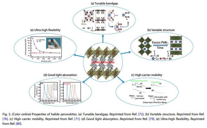
“And HPs are well-suited for memristor applica- tions because their mixed ion–electron conduction behavior allows halide counterions to move under applied optical, electric, or thermal fields[26, 27] .” (Cao et al., 2020, p. 2)
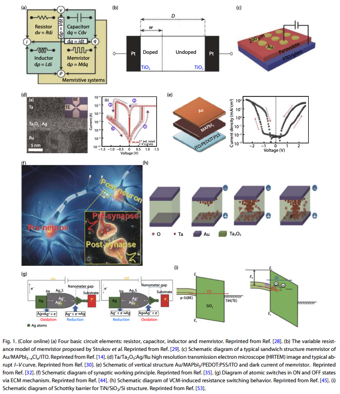
“In previous reports and studies, most memristor structures use the sandwich structure as shown in Fig. 1(c)[14] in which the metal is used as the bottom elec- trode (BE) and top electrode (TE), and functional layers con- sist of insulators, semiconductors, organics, or perovskites.” (Cao et al., 2020, p. 2)
“characteristics according to different mechanisms by apply- ing an external electric field, which can be divided into ab- rupt changes (Fig. 1(d)) and gradual changes (Fig. 1(e))[30-32] .” (Cao et al., 2020, p. 3)
“The resistive switching (RS) of the abrupt memristor (also called resistive random-access memory (RRAM)) is discrete, also known as a digital memristor. This type of memristor has multiple resistance states and can be developed for informa- tion storage and logic applications, where the stored informa- tion consists of different resistance states (high resistance state (HRS) and low resistance state (LRS))[33, 34].” (Cao et al., 2020, p. 3)
“The indicat- ors for measuring RRAM include threshold voltage distribu- tion, RHRS/RLRS ratio, retention, durability, and power consump- tion.” (Cao et al., 2020, p. 3)
“The resistance of the memristor with gradual changes is continuous, also known as the analog memristor. The conduct- ance of this type of memristor is continuously adjustable; thus, it behaves similarly to progressively continuous ad- justable synaptic weights in biological synapses. T” (Cao et al., 2020, p. 3)
“dρ = Mdq” (Cao et al., 2020, p. 3)
“Scientists have discovered that memris- tors can simulate biological synaptic functions, including spik- ing-time-dependent plasticity (STDP), paired-pulse facilita- tion (PPF), excitatory postsynaptic current (EPSC), short-term plasticity (STP), long-term plasticity (LTP), learning, and forget- ting[36-39].” (Cao et al., 2020, p. 4)
(Cao et al., 2020, p. 4) The physical mechanizm is strongly related to the electrode especially in the formation of conducting fillament. The electrode oxidized, difused, connect the top electrode and bottom electrod making abrupt change to low resistivity mode.
“There are two main types of physical mechanisms: formation and rupture of conductive filaments (CF) and interface types[41-43].” (Cao et al., 2020, p. 4)
“The formation and rupture of CF are mainly cau- sed by ion migration and redox reactions inside the material under the external electric field.” (Cao et al., 2020, p. 4)
“According to the type of mo- bile ions, the RS can be divided into electrochemical metalliza- tion (ECM) (Fig. 1(g))[44] and valence change mechanism (VCM) (Fig. 1(h))[45].” (Cao et al., 2020, p. 4)
“Memristors operated by ECM usually use
active metals as the TE (such as Ag and Cu). The migration of
active metal ions is a key factor causing RS[46, 47].” (Cao et al., 2020, p. 4) TE: top electrode
“When a posit- ive voltage is applied to the TE of the device, the active met- al is oxidized to cations. These cations continue to diffuse downward, passing through the functional layer under the drive of a positive electric field. Finally, the ions are reduced to metal at the BE, forming CF. The continuous growth of CF facilitates the communication between the TE and BE, and the memristor switches from HRS to LRS.” (Cao et al., 2020, p. 4)
“In contrast, when a negative voltage is applied, the memristor switches from LRS to HRS.” (Cao et al., 2020, p. 4)
“Selecting a functional layer material with excellent per- formance can effectively control the formation and rupture of CF[48, 49].” (Cao et al., 2020, p. 4)
“Another type of RS is caused by VCM in which the” (Cao et al., 2020, p. 4)
“memristor operates usually based on the migration and redis- tribution of anions, thereby changing the valence state of the functional layer material[45, 50].” (Cao et al., 2020, p. 4)
“To explain the RS behavior caused by VCM, we use metal oxide as a functional layer as an example to explain. When an electric field is applied, oxy- gen ions and oxygen vacancies (Vos) migrate. During the SET process (i.e., memristor switching from HRS to LRS), Vos accu- mulate towards the BE under the action of a positive electric field, resulting in the formation of CF of Vos. During the RE- SET process (memristor switching from LRS to HRS), Vos com- bine with oxygen ions, causing the CF to rupture[51, 52] .” (Cao et al., 2020, p. 4)
“Moreover, another type of physical mechanism that is a uni- form interface type physical mechanism (Fig. 1(i))[53], which is mainly caused by the Schottky barrier. The memristor function- al layer typically uses an insulator to build a Schottky contact point between the insulator and the electrode. The change in the Schottky barrier is usually accompanied by charge trap- ping/detrapping or anion migration at the insulating layer near the electrode[54, 55].” (Cao et al., 2020, p. 4)
“The conductive mechanism of memristors usually uses some models to fit the I–V curve, such as space charge-limited conduction (SCLC, I ∝ V2), Schottky emission (ln I ∝ V1/2), Poole-Frenkel emission (ln (I/V) ∝ V)1/2, trapped assisted tunneling (TAT, ln J ∝ 1/ E), thermionic emission (I ∝ V) and Fowler-Nordheim tunneling (FNT, ln (I/V2) ∝ 1/V)[56-59] .” (Cao et al., 2020, p. 4)
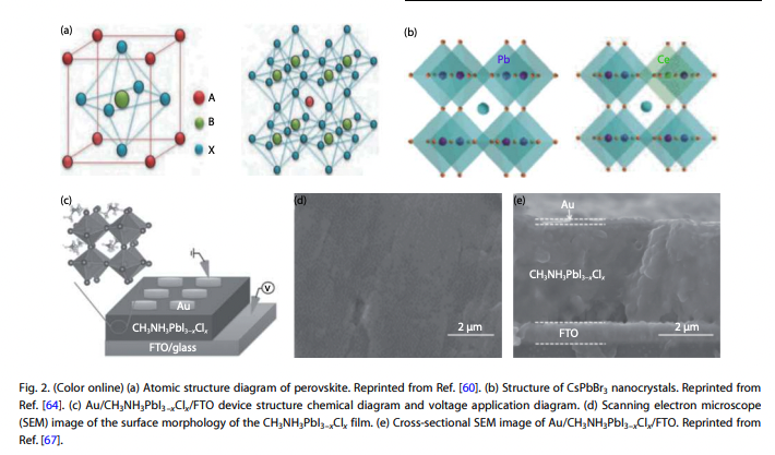
“Perovskite material is a compound with ABX3” (Cao et al., 2020, p. 4)
“A is a mono- valent cation and can be an organic (methylammonium CH3NH3 +) or inorganic (Cs+) cation. B is a divalent cation, such as Pb2+, Sn2+, and the like, and X is an anion.” (Cao et al., 2020, p. 4)
“when X is a hal- ide (I or Br), it is called an HP[61].” (Cao et al., 2020, p. 5)
“Inorganic HPs (Fig. 2(b))[64] are a class of func- tional materials with perovskite structure composed of inorgan- ic cations (alkaline earth metal cations), transition metals, and halogens.” (Cao et al., 2020, p. 5)
“It has been widely used as the functional layer in memristors and have shown excellent resistance-switching performance through tests[75] .” (Cao et al., 2020, p. 5)
“Choi et al. reported the first application of OHP materials (Au/CH3NH3PbI3-xClx/FTO) for non-volatile memory devices with significant RS effect[67] .
The device exhibits bipolar RS performance with a switching voltage of less than 1 V, which has been reported for the first time.” (Cao et al., 2020, p. 6)
“Sun et al. constructed a sandwich structure (ITO/PE- DOT:PSS/CH3NH3PbI3/C)[84]. The device has an on/off ratio of approximately 104 at a read voltage of 50 mV, which is the best result obtained from an OHP-based memristor.” (Cao et al., 2020, p. 6)
“Zou et al.
selected electrochemically active metal electrodes and suc-” (Cao et al., 2020, p. 6)
“cessfully prepared metal (Ag/Cu/Ti/Zn/Al)/CH3NH3PbClxI3-x/
TiO2 compact layer/FTO memristor devices[85].” (Cao et al., 2020, p. 6) Cek this refeerence:
Halide perovskite with various metal contacts
“It has a switch- ing current ratio as high as 1.9 × 10⁹, which is the highest value among all memristors reported so far. Such a high switching current ratio may result in faster read speeds, few- er errors, and lower power consumption.” (Cao et al., 2020, p. 6)
“In electrical memristors, the most critical properties are
switching speed, durability, retention, and power consump-
tion.” (Cao et al., 2020, p. 6) The most important properties in memristor are:
- Switching speed
- Durability
- Retention
- Power consumption
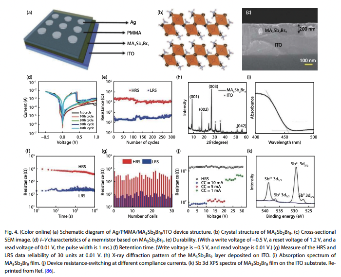
“In 2019,
Park et al. reported a lead-free perovskite-based material
(MA3Sb2Br9 (MA = CH3NH3)) for the resistive conversion of
memristors and neuromorphic computing with low energy
consumption[86]. In this paper, Ag/PMMA/MA3Sb2Br9/ITO
devices are demonstrated for the first time using MA3Sb2Br9
materials, as shown in Fig. 4(a).” (Cao et al., 2020, p. 6) PMMA :
Poly(methyl methacrylate)
named also acrylic / plexiglass
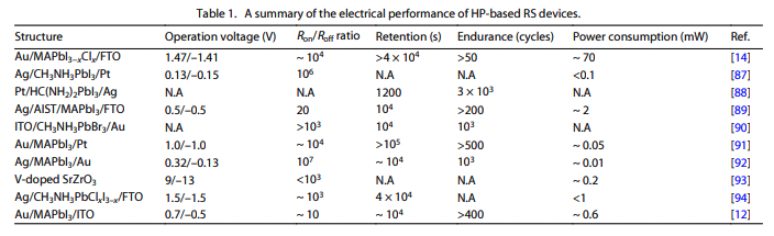
“Table 1 briefly summarizes the electrical perform-
ance of previous HP memristors.” (Cao et al., 2020, p. 6) This review paper summarize the electrical performance of Halide Perovskite memristor. Check.
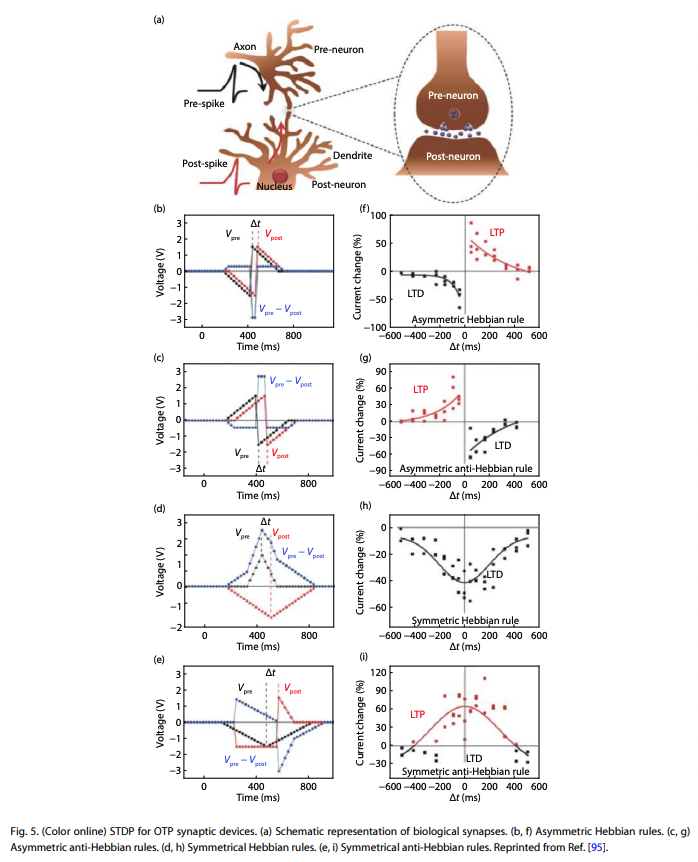
“Another important feature of memristors is that it can sim-
ulate biological synapses and prepare synaptic devices with
biomimetic functions. Park et al. simulated the EPSC, inhibit-
ory postsynaptic current, LTP, long-term depression (LTD),
and STDP using a device made of MA3Sb2Br9[86]. In 2016,
Huang et al. reported a synaptic device based on a two-termin-
al organometallic trihalide perovskite (OTP) with various func-
tions known in biological synapses, including STDP, spike
rate-dependent plasticity, STP, and LTP[95].” (Cao et al., 2020, p. 6) Want to know the application of perovskite memristor for biological synapses? Read these two papers.
“Biological syn-
apses transmit information between two nerve cells. The mem-
ristor BE and TEs serve as pre-synaptic and postsynaptic neur-
ons, respectively. The rate of change in device conductance in-
dicates the strength of the connection between neurons
(also called synaptic weight). In neuroscience, the tunability
of synaptic weight is called synaptic plasticity. Brain learning
and memory are mainly dependent on changes in synaptic
weight[39].” (Cao et al., 2020, p. 6) ### Synaptic weight
The rate of change in the conductance indicates the strength of the connection of the neuron. It is called synaptic weight. ### Synaptic plasticity
The tunability of this synaptic weight is called synaptic plasticity. Brain learning and memory are mainly dependent on changes in this synaptic weight.
“STDP (the Hebbian Learning Rule) refers to the” (Cao et al., 2020, p. 6) ### STPD
The Hebbian Learnign Rule.
The relation of the change of Synaptic Weight (
“When the postsynaptic spike reaches after the pre-synaptic spike (Δt > 0, Δt = tpost - tpre), the electrical conductivity in the artificial synaptic device increases, achieving LTP. Con- versely, if the postsynaptic is triggered before the pre-syn- aptic (∆t < 0), the synaptic weight is reduced, which results in LTD[96, 97].” (Cao et al., 2020, p. 7)
“Table 1. A summary of the electrical performance of HP-based RS devices.
Structure Operation voltage (V) Ron/Roff ratio Retention (s) Endurance (cycles) Power consumption (mW) Ref.
Au/MAPbI3-xClx/FTO 1.47/–1.41 ~ 104 >4 × 10⁴ >50 ~ 70 [14] Ag/CH3NH3PbI3/Pt 0.13/–0.15 106 N.A N.A <0.1 [87] Pt/HC(NH2)2PbI3/Ag N.A N.A 1200 3 × 10³ N.A [88] Ag/AIST/MAPbI3/FTO 0.5/–0.5 20 104 >200 ~ 2 [89] ITO/CH3NH3PbBr3/Au N.A >103 104 103 N.A [90] Au/MAPbI3/Pt 1.0/–1.0 ~ 104 >105 >500 ~ 0.05 [91] Ag/MAPbI3/Au 0.32/–0.13 107 ~ 104 103 ~ 0.01 [92] V-doped SrZrO3 9/–13 <103 N.A N.A ~ 0.2 [93] Ag/CH3NH3PbClxI3–x/FTO 1.5/–1.5 ~ 103 4 × 10⁴ N.A <1 [94] Au/MAPbI3/ITO 0.7/–0.5 ~ 10 ~ 104 >400 ~ 0.6 [12]” (Cao et al., 2020, p. 7)
“Huang et al. reported a mem- ristor application based on organic trihalide perovskite (OTP) materials in vertical and horizontal directions, the direction of photocurrent can be switched repeatedly by applying an elec- tric field of less than 1 V/𝜇m[32].” (Cao et al., 2020, p. 8)
“Sun et al. demonstrated that organic–inorganic hybrid perovskite materials can be used as a base material for non-volatile memristors with photo-responsive properties in the new sandwich structure[84].” (Cao et al., 2020, p. 8)
“Wu et al. reported for the first time the successful preparation of Ni/ZnO/CsPbBr3/FTO memristors based on the stability and high-performance of inorganic HP (CsPbBr3)[104]. Through the heterojunction between CsPbBr3 and ZnO, the device has a photo-sensing effect of more than 103 and a fast response speed (< 1 ms), allowing us to adjust the resistance state by simultaneously changing light and electric fields at the same time.” (Cao et al., 2020, p. 9)
“OHP has attracted increasing attention as a promising materi- al for memristors. In particular, their ion-electron conductiv- ity combined with photosensitivity provides OHP with the op- portunity to demonstrate novel functions, such as synaptic function of light and optical erasure memory[105-107].” (Cao et al., 2020, p. 9)
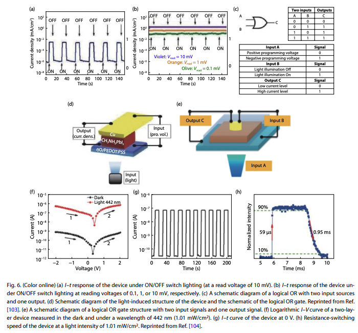
“sandwich structure ITO/PEDOT:PSS/CH3NH3PbI3/Cu to measure the light response performance of the device un- der HRS and LRS, as shown in Figs. 6(a)–6(d)[103]. The device current density can be transformed from 10-6 to 10-3 mA/ cm2, and the light response Ion/Ioff ratio is greater than 103 .” (Cao et al., 2020, p. 9)
“Based on this prin- ciple, a photosensitive logic OR gate with two inputs (A is the electric field and B is the light) and one output (C is the cur- rent) is designed. For the input signal A, we define the posit- ive voltage as "0" and the negative voltage as "1". For the in- put signal B, dark is represented as "0", and light is represen- ted as "1". The low current of the output signal C is the sig- nal "0", and the high current is the signal "1". For this ITO/PE- DOT: PSS/CH3NH3PbI3/Cu device, if one or both of the inputs are signal "1", the output is always signal "1". In contrast, only two inputs are signal "0" and the output is signal "0".” (Cao et al., 2020, p. 9)
“According to the band arrangement of ZnO
and CsPbBr3, Wu et al. designed the experiment to form a het-
erojunction at the ZnO/CsPbBr3 interface, which can realize
photovoltaic generation under illumination[104].” (Cao et al., 2020, p. 10) The resistivity change depending on/off of the light.
“And the current increases rapidly after lighting, the
on/off ratio is about 103. Response time was researched by us-
ing a trigger-assisted 442 nm continuous wave laser with ad-
justable pulse width. A 200 Hz pulse width was applied to
the device to test the rise time and decay time, and finally ob-
tained a rise time of 59 𝜇s and a fall time of 0.95 ms, indicat-
ing that the device has fast RS characteristics.” (Cao et al., 2020, p. 10) They test the responsiveness of the R change using pulse light. At 200 Hz
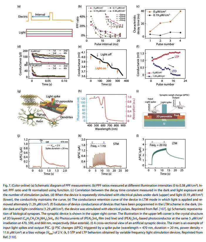
“Xie et al. studied the photoelectric synaptic plasticity of 2D lead- free perovskite ((PEA)2SnI4), as shown in Figs. 7(g)–7(l)[110] .
These devices show photocurrent activation of photo-stimula- tion in a manner similar to neurons and exhibit some syn- aptic bionic functions, such as STP, LTP, and spike-frequency- based transmission control. The strength of synaptic connec- tions can be effectively adjusted by the three elements of light (duration, wavelength, and irradiance).” (Cao et al., 2020, p. 10)
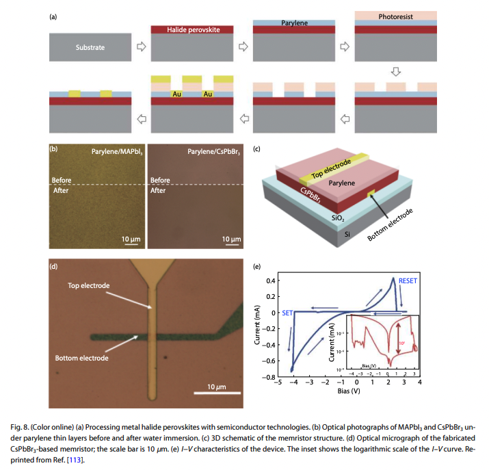
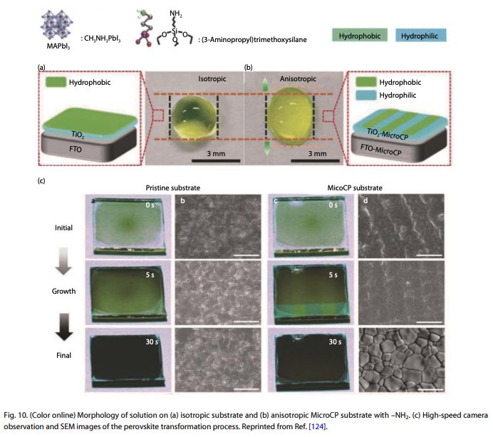
“The preparation methods of per- ovskite-type compounds mainly include the traditional high temperature solid-phase method, sol-gel method, hydrotherm-” (Cao et al., 2020, p. 10)
“al synthesis method, precipitation method, and vapor depos- ition method. I” (Cao et al., 2020, p. 10)
“Cheng et al. successfully prepared a MAPbI3 photodetector and a CsPbBr3 memristor with the aid of a parylene as a waterproof layer of a perovskite materi- al[113].” (Cao et al., 2020, p. 10)
“The optical photos of the MAPbI3 or CsPbBr3 film protected with parylene be- fore and after the 1 h water immersion process are shown in Fig. 8(b). It can be seen that MAPbI3 or CsPbBr3 is not dis- solved, indicating that parylene can protect the perovskite ma- terial.” (Cao et al., 2020, p. 10)
(Cao et al., 2020, p. 12)
(Cao et al., 2020, p. 12) LRS->HRS
- At positive voltage
- Reset HRS->LRS
- the opposite
What is Neumann bottleneck
The Neumann bottleneck is a concept in artificial intelligence (AI) that states that for any problem-solving system, the speed of problem-solving is ultimately constrained by the speed of the system's ability to represent and manipulate symbols. This idea was originally proposed by mathematician and computer scientist John von Neumann in 1945. The bottleneck is caused by the time it takes for a computer to access and manipulate data—a process known as computation. As computers become faster, they may be able to process more data more quickly, but they will still be limited by their ability to represent and manipulate symbols.
Make summary
This paper studies the application of halide perovskites in optoelectronic devices such as solar cells, light-emitting diodes (LEDs), and photodetectors. It examines the structure, properties, and performance of halide perovskites to understand how they can be utilized in optoelectronic devices. The paper reviews various device structures that have been developed with halide perovskites, along with their advantages and disadvantages. It also discusses current challenges associated with using these materials and ways to overcome them. The paper provides a comprehensive overview of the current state of research on halide perovskite application in optoelectronic devices, offering insight into potential future directions for research and development in this field.